Backlight structure and display device

A backlight structure and display device technology, applied in optics, nonlinear optics, instruments, etc., can solve the problem of optical fingerprint optical path design in the display area. The sensor arrangement has great difficulty, low transmittance, and has not been introduced under a reasonable LCD screen. Fingerprints etc.

Active Publication Date: 2020-03-06
WUHAN CHINA STAR OPTOELECTRONICS TECH CO LTD
View PDF8 Cites 4 Cited by
  • Summary
  • Abstract
  • Description
  • Claims
  • Application Information

AI Technical Summary

Problems solved by technology

[0002] The fingerprint recognition technology under the optical screen is currently becoming a hot spot in the market. Due to the low penetration rate of the liquid crystal display (Liquid Crystal Display), the dimming function of the liquid crystal light valve and the relatively complex stacked structure, optical fingerprints are performed in the display area. Optical path design and sensor arrangement are more difficult
At present, there is no reasonable and commercially available fingerprint recognition technology under the LCD screen on the market

Method used


Image

  • Backlight structure and display device
  • Backlight structure and display device
  • Backlight structure and display device

Examples


Embodiment Construction

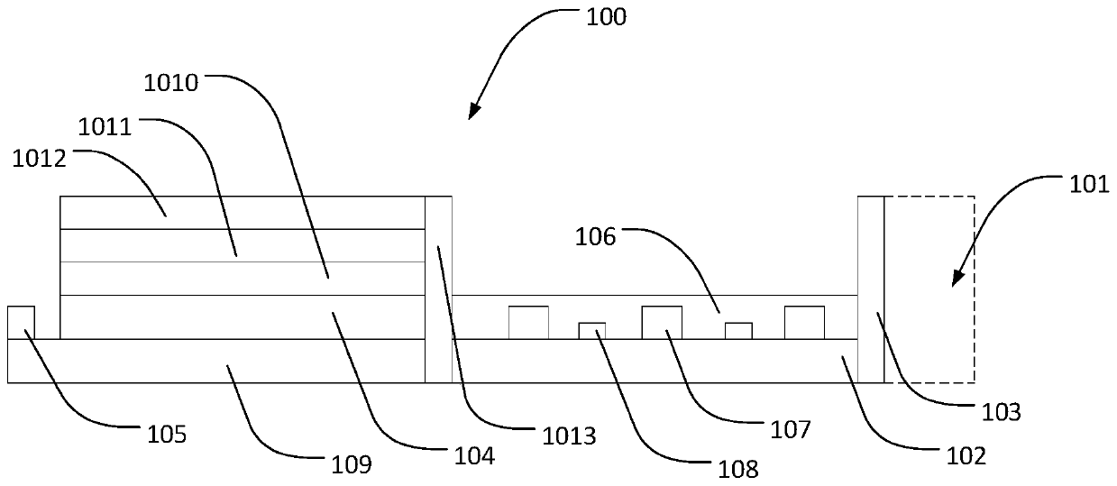
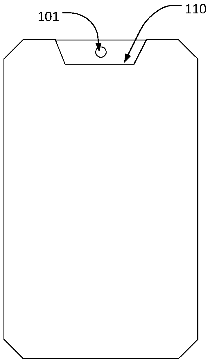
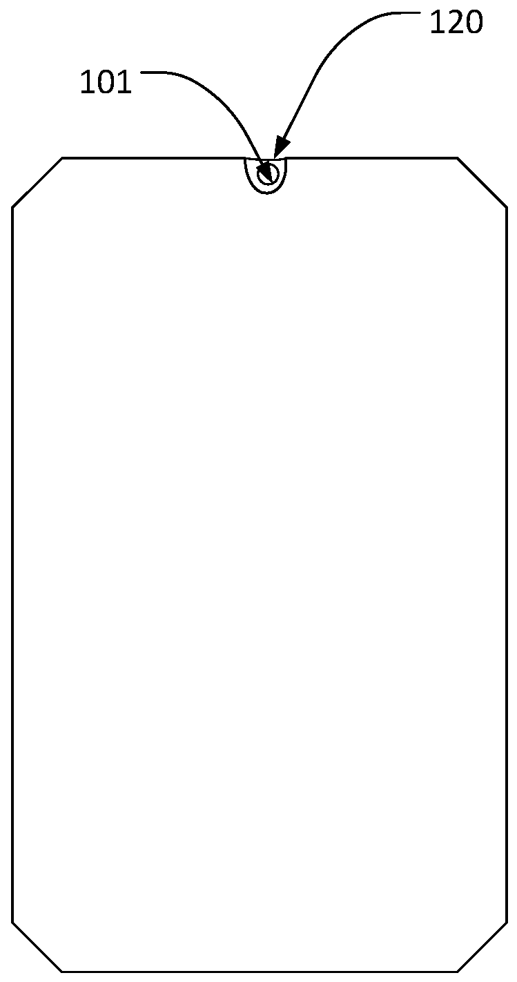
[0032] The following descriptions of the various embodiments refer to the accompanying drawings to illustrate specific embodiments in which the present invention may be practiced. The directional terms mentioned in the present invention, such as up, down, front, back, left, right, inside, outside, side, etc., are only directions referring to the drawings. The component names mentioned in the present invention, such as first, second, etc., are only used to distinguish different components, which can be better expressed. In the figures, structurally similar elements are denoted by the same reference numerals.

[0033] Embodiments of the present invention will be described in detail herein with reference to the accompanying drawings. This invention may be embodied in many different forms and should not be construed as only the specific embodiments set forth herein. These embodiments are provided to explain the practical application of the invention, so that others skilled in th...


PUM


Abstract

The present invention provides a backlight structure and a display device. MiniLed light emitting units are arranged around the light holes of the backlight structure, and fingerprint photosensitive chips are arranged between the MiniLed light emitting units, so that fingerprint identification around the light holes can be realized. According to the display device, when a display function needs tobe started, the MiniLed light emitting units are used as a backlight source in the special-shaped area, and simple picture display of the special-shaped area can be achieved through dimming of a liquid crystal box above the backlight structure and a light gathering and guiding ring above the light holes. When a photographing function needs to be started, the MiniLed light emitting units are closed, and the liquid crystal box is in a transparent state, so that light enters a camera for photographing. When a fingerprint unlocking function needs to be started, the liquid crystal box at the upperportion is transparent, corresponding single-color Mini Led (a red light emitting unit, a green light emitting unit and a blue light emitting unit) is started according to visible light wave bands (red light, green light or blue light) which can be recognized by the fingerprint photosensitive chip, and after unlocking succeeds, the single-color MiniLed is closed, and the special-shaped area display function is normally started.

Description

technical field [0001] The invention relates to the field of display technology, in particular to a backlight structure and a display device. Background technique [0002] The fingerprint recognition technology under the optical screen is currently becoming a hot spot in the market. Due to the low penetration rate of the liquid crystal display (Liquid Crystal Display), the dimming function of the liquid crystal light valve and the relatively complex stacked structure, optical fingerprints are performed in the display area. Optical path design and sensor arrangement are more difficult. At present, there is no reasonable and commercially available fingerprint recognition technology under the LCD screen on the market. Under-screen optical fingerprint recognition technology, as a pre-research technology for the combination of artificial intelligence and display technology, is favored by many manufacturers. How to design a reasonable optical fingerprint light path and mechanism...

Claims


Application Information

Patent Timeline
Patent Type & Authority Applications(China)
IPC IPC(8): G02F1/13357G02F1/1333G06K9/00
CPCG02F1/133615G02F1/13338G06V40/13
Inventor 杨勇
Owner WUHAN CHINA STAR OPTOELECTRONICS TECH CO LTD
Why Eureka
Try Eureka