Liquid crystal display panel and display device

A liquid crystal display panel and liquid crystal layer technology, applied in optics, instruments, electrical digital data processing, etc., can solve the problems of increasing the difficulty of integrating the optical fingerprint recognition function of the liquid crystal screen, and achieve the goal of increasing the aperture ratio, reducing noise, and reducing interference Effect

Active Publication Date: 2021-04-16
WUHAN CHINA STAR OPTOELECTRONICS TECH CO LTD
View PDF8 Cites 1 Cited by
  • Summary
  • Abstract
  • Description
  • Claims
  • Application Information

AI Technical Summary

Problems solved by technology

[0007] The purpose of the present invention is to provide a liquid crystal display panel and a display device to solve the technical problem that the limitation of factors such as backlight and aperture ratio increases the difficulty of integrating the optical fingerprint recognition function inside the liquid crystal screen

Method used


Image

  • Liquid crystal display panel and display device
  • Liquid crystal display panel and display device
  • Liquid crystal display panel and display device

Examples


Embodiment 1

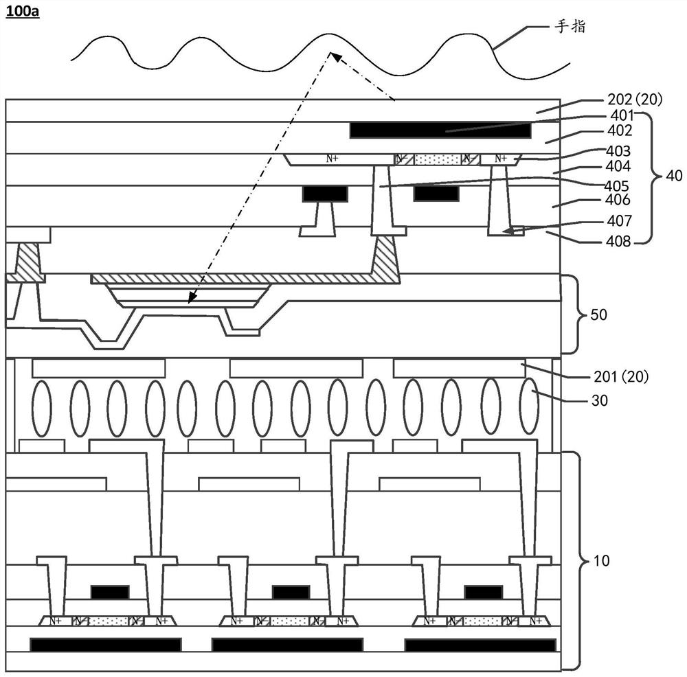
[0045] Such as figure 1 as shown, figure 1 It is a schematic structural diagram of the liquid crystal display panel provided in Embodiment 1 of the present application.

[0046] This embodiment provides a liquid crystal display panel 100a, the liquid crystal display panel 100a includes a color filter substrate 10 , an array substrate 10 , a liquid crystal layer 30 , a fingerprint driving circuit structural layer 40 and a fingerprint sensor structural layer 50 . Wherein, the color filter substrate 10 is arranged opposite to the array substrate 10, the liquid crystal layer 30 is arranged between the color filter substrate 10 and the array substrate 10, the fingerprint driving circuit structure layer 40 and the The fingerprint sensor structure layer 50 is disposed in the color filter substrate 10 , and the fingerprint driving circuit structure layer 40 is used to provide a driving voltage for the fingerprint sensor 50 .

[0047] Such as figure 2 as shown, figure 2 It is a s...

Embodiment 2

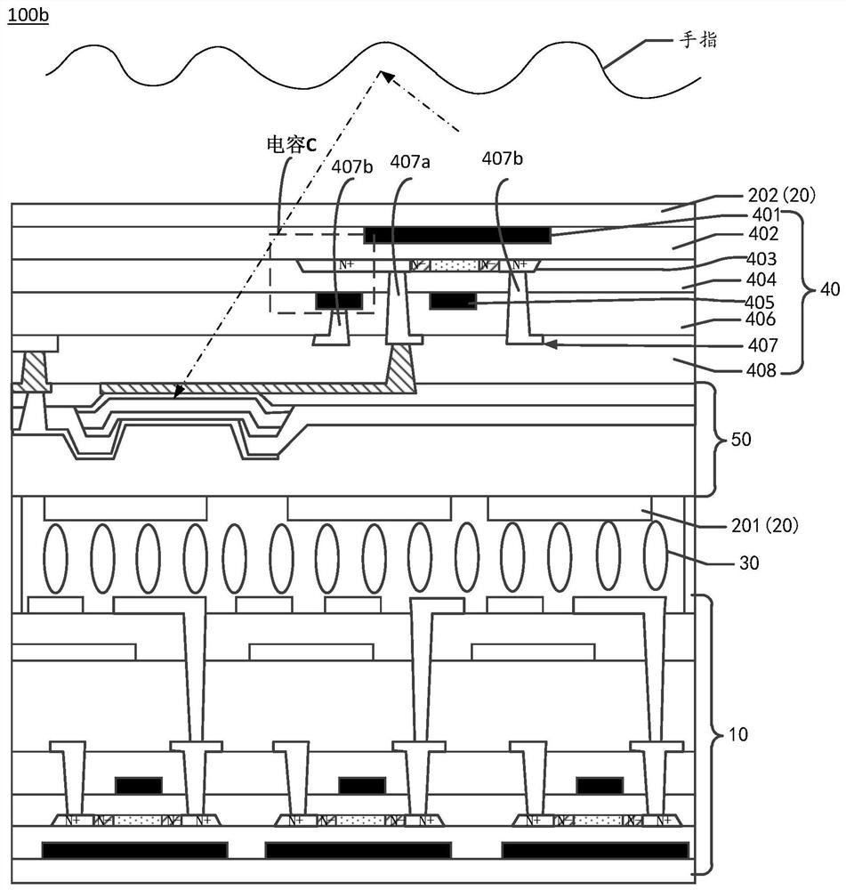
[0067] Such as image 3 as shown, image 3 It is a schematic structural diagram of a liquid crystal display panel provided in Embodiment 2 of the present application.

[0068] This embodiment provides a liquid crystal display panel 100b, the liquid crystal display panel 100b includes most of the technical solutions of the first embodiment, the difference is that the fingerprint sensor structure layer 50 further includes a third passivation layer.

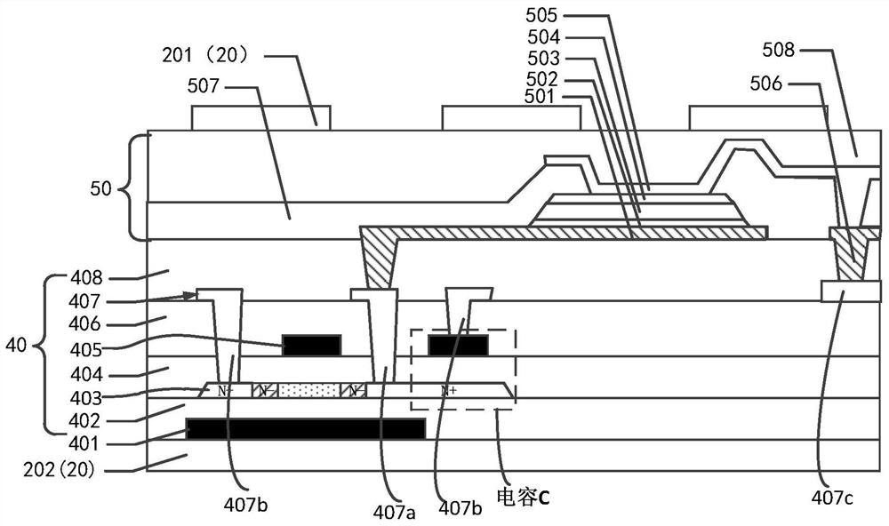
[0069] Such as Figure 4 as shown, Figure 4 It is a schematic structural diagram of the color filter substrate side of the liquid crystal display panel provided in Embodiment 2 of the present application.

[0070] Specifically, the common electrode 506 is disposed on the same layer as the first electrode 501 and connected to the data wiring 407c.

[0071] The second passivation layer 507 covers part of the first electrode 501 and the common electrode 506, and extends to the surface of the first passivation layer 408, wherein th...

Embodiment 3

[0076] Such as Figure 5 as shown, Figure 5 It is a schematic structural diagram of a liquid crystal display panel provided in Embodiment 3 of the present application.

[0077] This embodiment provides a liquid crystal display panel 100a, the liquid crystal display panel 100a includes a color filter substrate 20 , an array substrate 10 , a liquid crystal layer 30 , a fingerprint driving circuit structural layer 40 and a fingerprint sensor structural layer 50 . Wherein, the color filter substrate 20 is arranged opposite to the array substrate 10, the liquid crystal layer 30 is arranged between the color filter substrate 20 and the array substrate 10, the fingerprint drive circuit structure layer 50 and the The fingerprint sensor structural layer 50 is disposed on a side of the color filter substrate 20 away from the liquid crystal layer 30 , and the fingerprint driving circuit structural layer 40 is used to provide a driving voltage for the fingerprint sensor 50 .

[0078] W...


PUM


Abstract

The invention discloses a liquid crystal display panel and a display device. The liquid crystal display panel comprises: an array substrate; a color film substrate arranged opposite to the array substrate; a liquid crystal layer arranged between the array substrate and the color film substrate; and a fingerprint driving circuit structure layer and the fingerprint sensor structure layer which are both arranged in the color film substrate or are both arranged on the side, away from the liquid crystal layer, of the color film substrate. The fingerprint driving circuit structure layer is used for providing driving voltage for the fingerprint sensor. Interference of liquid crystal in the liquid crystal layer on finger reflection can be reduced, and noise is lowered.

Description

technical field [0001] The present application relates to the field of display technology, in particular to a liquid crystal display panel and a display device. Background technique [0002] With the development of electronic technology, fingerprint identification technology has been widely used in small and medium-sized panels, mainly including capacitive, ultrasonic and optical methods. [0003] At present, the relatively mature scheme is capacitive fingerprint recognition. Its working principle is to use the silicon wafer and the conductive subcutaneous electrolyte to form an electric field. fingerprint determination. However, for capacitive fingerprint recognition, when the finger is wet, the detection effect will be significantly worse. Compared with capacitive fingerprint recognition technology, ultrasonic fingerprint recognition technology has the advantages of high penetrating ability, more stable and more accurate, but its cost is relatively high. Optical fingerp...

Claims


Application Information

Patent Timeline
IPC IPC(8): G02F1/1333G02F1/1335G06F3/041G06F3/042
Inventor 宋继越艾飞宋德伟
Owner WUHAN CHINA STAR OPTOELECTRONICS TECH CO LTD
Why Eureka
Try Eureka