Supercharge Your Innovation With Domain-Expert AI Agents!

Electronic device and process of forming the same

A technology of electronic devices and terminals, which is applied in the field of electronic devices and their formation, and can solve the problem of difficulty in controlling the shape of the field stop region

Pending Publication Date: 2020-03-17
SEMICON COMPONENTS IND LLC
View PDF5 Cites 0 Cited by
  • Summary
  • Abstract
  • Description
  • Claims
  • Application Information

AI Technical Summary

Problems solved by technology

Therefore, the above method can make it difficult to control the shape of the field stop region

Method used


Image

  • Electronic device and process of forming the same
  • Electronic device and process of forming the same
  • Electronic device and process of forming the same

Examples


Embodiment approach 1

[0061] Embodiment 1. An electronic device which may comprise:

[0062] A semiconductor substrate having a first main side, a second main side opposite the first main side, and a second main surface along the second main side;

[0063] an emitter region closer to the first main side than to the second main side, wherein the emitter region has a first conductivity type;

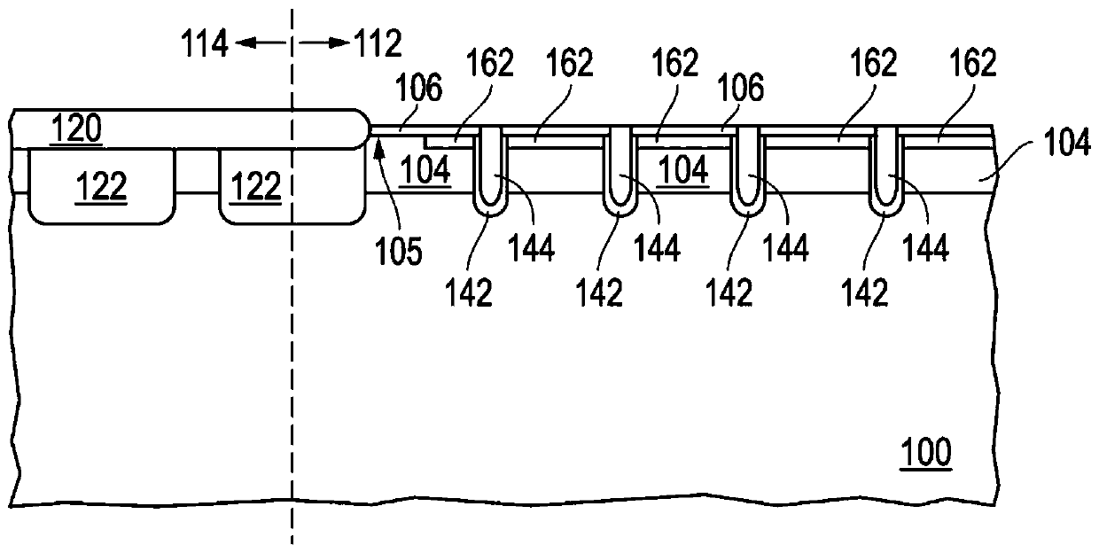
[0064] a trench extending from the second main surface into the semiconductor substrate, wherein the trench has sidewalls and a bottom;

[0065] a collector region spaced along the second major surface and from the bottom of the trench, wherein the collector region has a second conductivity type opposite the first conductivity type;

[0066] a field stop region disposed along at least a portion of the bottom and sidewalls of the trench, wherein the field stop region has the first conductivity type; and

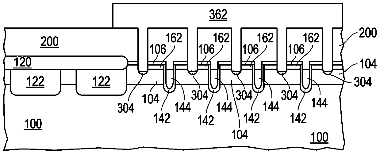
[0067] A collector terminal along the second major side and comprising a metal-containing material, wherei...

Embodiment approach 2

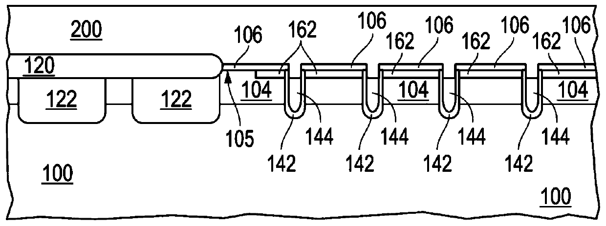
[0068] Embodiment 2. The electronic device of Embodiment 1, further comprising an insulating layer disposed along sidewalls and a bottom of the trench, wherein the insulating layer is disposed between the field stop region and the collector terminal.

Embodiment approach 3

[0069] Embodiment 3. The electronic device of Embodiment 2, wherein the insulating layer substantially fills the trench.


PUM

PropertyMeasurementUnit
thicknessaaaaaaaaaa

Abstract

An electronic device and a process of forming the same are provided. The electronic device can include a semiconductor substrate having a front side and a back side; an emitter region closer to the front side than to the back side; a trench extending from a back side surface into the semiconductor substrate, with the trench having a sidewall and a bottom; a collector region along the back side surface and spaced apart from the bottom of the trench; a field-stop region lying along the bottom and at least a portion of the sidewall of the trench, wherein the emitter and field-stop regions have one conductivity type, and the collector region has the opposite conductivity type; and a collector terminal along the back side and including a metal-containing material, wherein the collector terminalcontacts the collector region and is isolated from the field-stop region.

Description

technical field [0001] The present disclosure relates to electronic devices and methods of forming electronic devices, and more particularly, to electronic devices including insulated gate bipolar transistors having field stop regions and methods of forming the same. Background technique [0002] An insulated gate bipolar transistor may have a field stop region adjacent to the collector region. The field stop region has a conductivity type opposite to that of the collector region. The field stop region can provide a more gradual rate of change of the emitter-to-collector voltage at relatively higher voltages during switching operations. Relatively deep field stop regions are desirable; however, conventional approaches may have adverse consequences. For example, a silicon-on-insulator approach may have field stop regions within the initial starting wafer. This approach has quality problems near the edges of the bonded substrates. Another approach may involve a buried laye...

Claims


Application Information

Patent Timeline
Patent Type & Authority Applications(China)
IPC IPC(8): H01L29/06H01L29/417H01L29/739H01L21/331
CPCH01L29/7393H01L29/0684H01L29/41708H01L29/66325H01L29/66348H01L29/7397H01L29/083H01L29/0623H01L29/7396H01L29/1095H01L29/0615H01L21/26586
Inventor 李孟家R·N·瓦尔
Owner SEMICON COMPONENTS IND LLC
Features
  • R&D
  • Intellectual Property
  • Life Sciences
  • Materials
  • Tech Scout
  • Unparalleled Data Quality
  • Higher Quality Content
  • 60% Fewer Hallucinations
Learn More