

Array substrate, preparation method thereof and display panel
An array substrate and substrate substrate technology, which is applied in the manufacture of semiconductor/solid-state devices, semiconductor devices, electrical components, etc., can solve the problems of poor TFT stability, uneven display screen, start-up voltage drift, etc., to improve working stability, Avoid short circuits and improve user experience
- Summary
- Abstract
- Description
- Claims
- Application Information
AI Technical Summary
Problems solved by technology
Method used
Image

Examples
Embodiment Construction
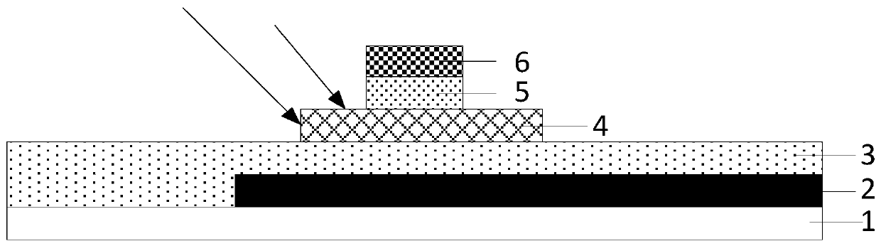
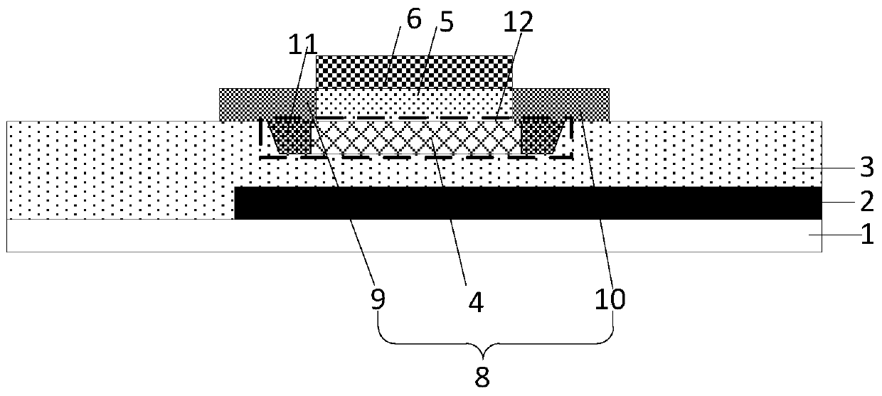
[0063] The embodiment of the present application provides an array substrate, such as figure 2 As shown, the array substrate includes: a base substrate 1, a light-shielding layer 2 on the base substrate 1, a buffer layer 3 on the light-shielding layer 2, and a buffer layer 3 on the buffer layer 3. a source layer 8, and a light shielding portion 11; the buffer layer 3 has a groove 12;
[0064] The active layer 8 includes: a semiconductor region 4, and a first conductorized region 9 and a second conductorized region 10 of the semiconductor region 4;
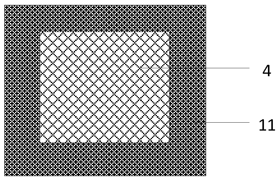
[0065] The semiconductor region 4 and the light shielding portion 11 fill the groove 12; as image 3 As shown, the shape of the orthographic projection of the light-shielding portion 11 on the base substrate 1 is ring-shaped, the side surface of the semiconductor region 4 is completely surrounded by the light-shielding portion 11, the first conductive region 9 and the The second conductive region 10 is located on the light shiel...
PUM
 Abstract
Description
Claims
Application Information