Light emitting device, display device, method of manufacturing display device, and power generation device

A technology for light-emitting devices and display devices, which is applied in semiconductor/solid-state device manufacturing, electric solid-state devices, semiconductor devices, etc., can solve the problems that there are no diversified quantum dot display device structures, simple layer structures, etc., and is suitable for large-scale The effect of simple production and processing technology and broad market prospects

Inactive Publication Date: 2020-06-05
TCL CORPORATION
View PDF5 Cites 0 Cited by
  • Summary
  • Abstract
  • Description
  • Claims
  • Application Information

AI Technical Summary

Problems solved by technology

[0004] However, the current quantum dot display devices are all film-layer structures, and the layer structure is relatively simple except for materials, and there is no diversified quantum dot display device structure yet.

Method used


Image

  • Light emitting device, display device, method of manufacturing display device, and power generation device
  • Light emitting device, display device, method of manufacturing display device, and power generation device
  • Light emitting device, display device, method of manufacturing display device, and power generation device

Examples


Embodiment 1

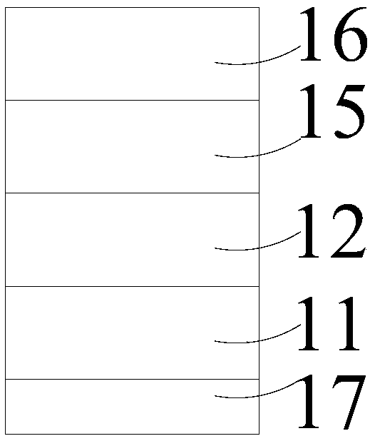
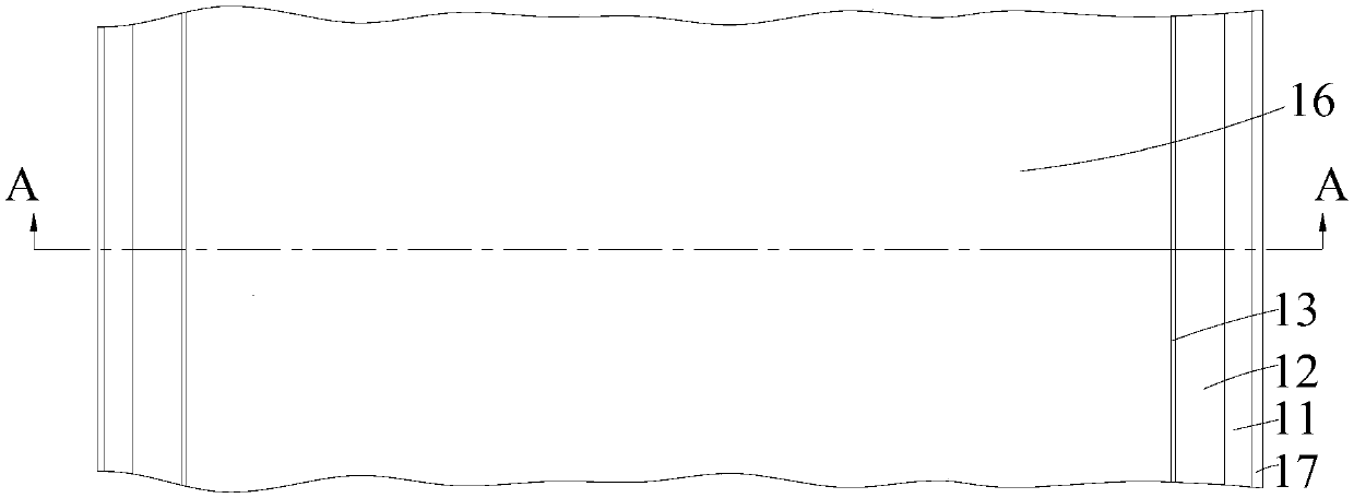
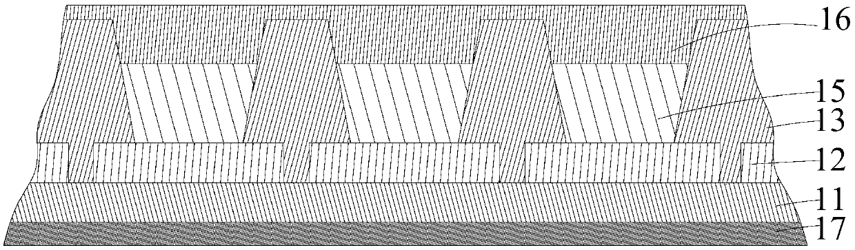
[0139] Such as Figure 21 As shown, a display device includes a light source 17, a substrate 11, an anode 12, a pixel defining layer 13, a core function layer 15 (also called a light-emitting layer), and a cathode 16; wherein, the substrate 11 is a transparent glass plate, and the anode 12 The material of the pixel definition layer 13 is silicon dioxide, the material of the core functional layer 15 is a mixture of CdSe / ZnS quantum dots and silicon dioxide, and the material of the cathode 16 is AZO.

[0140] see Figure 11-21 , the manufacturing method of the light-emitting display device is as follows:

[0141] S1. provide liner 11, this substrate 11 has opposite first surface and second surface, on the first surface of substrate 11, prepare a number of anodes 12 that are side by side and have intervals, at the edge of described anode 12 and by interval A pixel defining layer 13 is prepared on the exposed first surface of the substrate 11, and a pixel groove 14 is formed sur...


PUM

PropertyMeasurementUnit
thicknessaaaaaaaaaa

Abstract

The invention relates to the technical field of photoelectricity, and particularly provides a light emitting device, a display device, a method of manufacturing the display device and a power generation device. The light emitting device comprises a light source, a substrate and a core function unit, wherein the substrate is arranged between the light source and the core function unit, the core function unit comprises an anode, a core function layer and a cathode, the core function layer is arranged between the anode and the cathode, and the material of the core function layer is formed by mixing nanoparticles and a semiconductor material. The light emitting device provided by the invention can realize effective adjustment of light emitting brightness so as to obtain light emitting effectswith different brightness requirements. According to the display device based on the light emitting device, the brightness of each pixel unit can be adjusted, so that effective display is formed, andthe structure and the application of the light emitting display device are greatly expanded.

Description

technical field [0001] The invention belongs to the field of optoelectronic technology, and in particular relates to a light emitting device, a display device, a manufacturing method of the display device and a power generating device. Background technique [0002] As a luminescent material, colloidal quantum dots (Quantum dots, QDs) have incomparable advantages over other luminescent materials, such as continuously adjustable luminous wavelength, ultra-high internal quantum efficiency, and excellent color purity. It has great application prospect. Due to the optical properties of the material, quantum dots are used in LCD panels to enhance the color gamut. At the same time, with the deepening of quantum dot electroluminescence (quantum dot light-emitting diode, QLED) research, more and more progress has been made in the industrialization process. [0003] At present, the quantum dot display technology on the market mainly uses the principle of quantum dot photoluminescenc...

Claims


Application Information

Patent Timeline
Patent Type & Authority Applications(China)
IPC IPC(8): H01L51/50H01L51/56
CPCH10K50/115H10K71/00
Inventor 曹蔚然钱磊
Owner TCL CORPORATION
Why Eureka
Try Eureka