
Method, device, storage medium and terminal for identifying laser fault injection attack

A fault injection and laser technology, which is applied in the countermeasures of attacking encryption mechanisms, secure communication devices, digital transmission systems, etc., to achieve the effect of using less resources, providing security, and wide application.

Active Publication Date: 2021-03-26
GREE ELECTRIC APPLIANCES INC +1
View PDF7 Cites 0 Cited by
  • Summary
  • Abstract
  • Description
  • Claims
  • Application Information

AI Technical Summary

Problems solved by technology

[0005] The object of the present invention is to, aiming at the above defects, provide a method, device, storage medium and terminal for identifying laser fault injection attacks, to solve the problem of identifying whether the chip has been attacked by laser fault injection in the prior art, and to achieve The effect of protecting the configuration information

Method used


Image

  • Method, device, storage medium and terminal for identifying laser fault injection attack
  • Method, device, storage medium and terminal for identifying laser fault injection attack
  • Method, device, storage medium and terminal for identifying laser fault injection attack

Examples


Embodiment 1

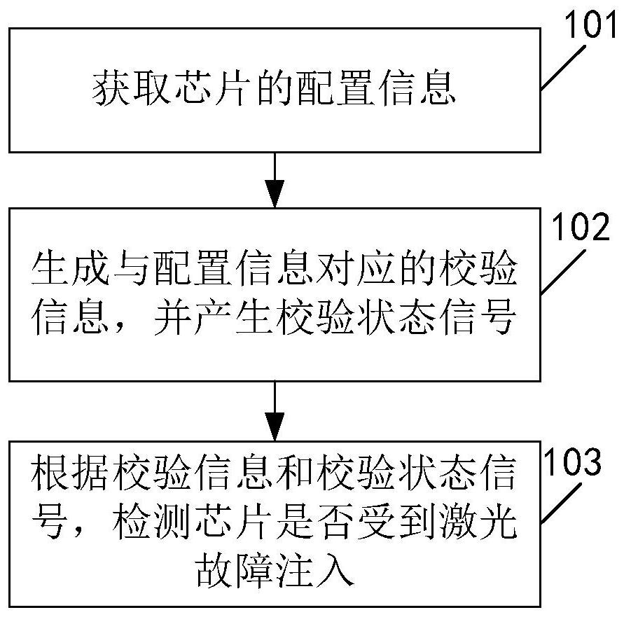
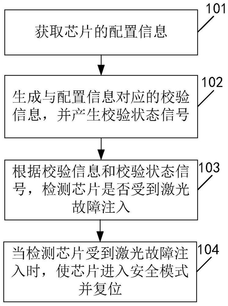
[0063] see figure 1 , an embodiment of the present invention provides a method for identifying a laser fault injection attack, the method for identifying a laser fault injection attack may include:

[0064] 101: Obtain configuration information of the chip.

[0065] Among them, the configuration information of the chip is used to distinguish the product direction, characteristics, etc. to apply to different application scenarios, and the configuration information is usually stored in NVM (Non-volatile memory, non-volatile memory). Configuration information also includes some sensitive configuration information that can be used as a condition for enabling or disabling special functions of the chip.

[0066] Specifically, obtain the configuration information of the chip, including:

[0067] Obtain the configuration information update enable signal (cfg_upd_en) generated by the preset enable signal control module;

[0068] Read the configuration information of the chip from NV...

Embodiment 2

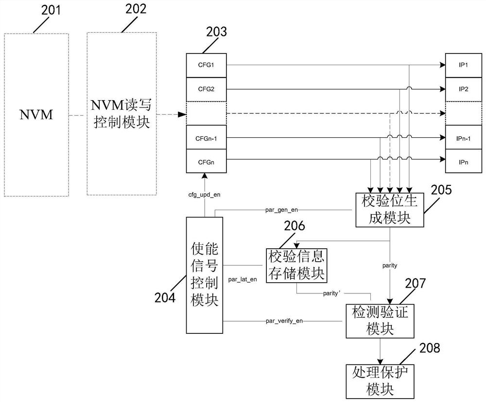
[0095] For ease of understanding, see image 3 and Figure 4 , the embodiment of the present invention is further described with a specific example, image 3 The meaning of each module in is as follows:

[0096] NVM (non-volatile memory) 201 is used to store configuration information and other information of the chip. The configuration information includes sensitive configuration information.

[0097] An NVM read and write control module (NVM glue logic) 202 is used to complete operations such as programming, erasing, and reading of NVM.

[0098] The register group 203 is used to latch the configuration information read from the NVM by the NVM read / write control module.

[0099] The enable signal control module 204 is configured to generate a configuration information update enable signal (cfg_upd_en), a check information generation enable signal (par_gen_en), a check information latch enable signal (par_lat_en) and a check enable signal (par_verify_en ), start the operat...

Embodiment 3

[0131] see Figure 5 , an embodiment of the present invention provides a device for identifying a laser fault injection attack, the device for identifying a laser fault injection attack may include:

[0132] An acquisition module 401, configured to acquire configuration information of the chip;

[0133] A parity generation module 402, configured to generate parity information corresponding to the configuration information, and generate

[0134] Verify status signal;


PUM


Abstract

The invention discloses a method and a device for identifying a laser fault injection attack, a storage medium and a terminal. The method comprises the following steps: acquiring configuration information of a chip; generating verification information corresponding to the configuration information, and generating a verification state signal; and detecting whether the chip is subjected to laser fault injection or not according to the verification information and the verification state signal. The device comprises an acquisition module, a check bit generation module and a detection verificationmodule. According to the scheme of the invention, whether the chip is attacked or not can be identified by detecting whether the chip is subjected to laser fault injection or not according to the generated verification information corresponding to the configuration information and the verification state signal, so that the configuration information in the chip can be protected, and heavy loss is avoided.

Description

technical field [0001] The invention belongs to the technical field of electronic computers, and in particular relates to a method, device, storage medium and terminal for identifying laser fault injection attacks, and in particular to a configuration information protection method, device, storage medium and terminal against laser attacks. Background technique [0002] Chips (also known as "integrated circuits") have a wide range of applications. In chip design, it is necessary to set corresponding configuration information for the chip according to the actual application scenario of the chip. Configuration information is used to distinguish product directions, features, etc. for different application scenarios, and configuration information is usually stored in NVM (Non-Volatile Memory, non-volatile memory). Some of the configuration information will be used as the conditions for enabling or disabling the special functions of the chip, and the configuration information corr...

Claims


Application Information

Patent Timeline
Patent Type & Authority Patents(China)
IPC IPC(8): H04L9/00G06F21/55
CPCG06F21/55H04L9/004
Inventor 温浪明陈恒张浩亮方励
Owner GREE ELECTRIC APPLIANCES INC
Learn More