Network-on-chip design method and device based on hybrid routing algorithm

An on-chip network and hybrid routing technology, applied in the computer field, can solve the problem of not being able to improve efficiency, and achieve the effects of improving efficiency, reducing data congestion, and improving performance

Active Publication Date: 2020-07-17
INSPUR SUZHOU INTELLIGENT TECH CO LTD
View PDF5 Cites 5 Cited by
  • Summary
  • Abstract
  • Description
  • Claims
  • Application Information

AI Technical Summary

Problems solved by technology

[0009] Existing technologies, whether using the basic XY routing algorithm or a specific optimized routing algorithm, regard the entire on-chip network as a unified whole. The optimization based on this idea is faced with large-scale asymmetric on-chip Uneven data transmission on the network often fails to improve overall efficiency

Method used


Image

  • Network-on-chip design method and device based on hybrid routing algorithm
  • Network-on-chip design method and device based on hybrid routing algorithm
  • Network-on-chip design method and device based on hybrid routing algorithm

Examples


Embodiment Construction

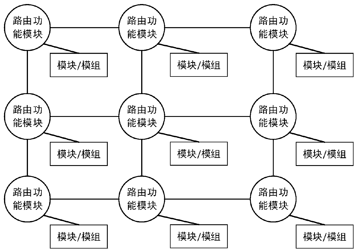
[0036]Embodiments of the present invention are described below. It is to be understood, however, that the disclosed embodiments are merely examples and that other embodiments may take various alternative forms. The figures are not necessarily to scale; some features may be exaggerated or minimized to show details of particular components. Therefore, specific structural and functional details disclosed herein are not to be interpreted as limiting, but merely as a representative basis for teaching one skilled in the art to variously employ the present invention. As will be understood by persons of ordinary skill in the art, various features shown and described with reference to any one figure can be combined with features shown in one or more other figures to create embodiments not explicitly shown or described . Combinations of features shown provide representative embodiments for typical applications. However, various combinations and modifications of the features consisten...


PUM


Abstract

The invention provides a network-on-chip design method and device based on a hybrid routing algorithm, and the method comprises the steps: dividing nodes into a controller node, a data processing node, a data exchange node and an equipment node according to the functional characteristics of the nodes in a network-on-chip; arranging the nodes from the central position of the network-on-chip to theperiphery layer by layer according to the sequence of the controller node, the data processing node, the data exchange node and the equipment node; and taking the controller node and the data processing node as a group, taking the data exchange node and the equipment node as another group, and adopting self-adaptive routing between each group, and adopting XY routing or YX routing between the groups. Based on data transmission characteristics and arrangement modes of different types of nodes, data transmission between different nodes is realized by using different routing algorithms, and the performance of the network-on-chip and the whole chip is improved.

Description

technical field [0001] The present invention relates to the computer field, and more specifically, relates to an on-chip network design method and device based on a hybrid routing algorithm. Background technique [0002] With the development of chip technology and the continuous increase in the complexity of application scenarios, for complex function chips that need to cope with complex scenarios, the implementation of a single architecture will cause too high complexity and dependence between different functions, thus greatly prolonging the development cycle. , it is difficult to meet the application requirements. This type of chip (such as mobile phone chips, general-purpose processor chips, AI chips, etc.) has begun to widely adopt an architecture that integrates multiple cores with different functions - different core modules focus on implementing and optimizing specific functions, and then use the bus Communication and collaboration to complete complete chip functions...

Claims


Application Information

Patent Timeline
Patent Type & Authority Applications(China)
IPC IPC(8): G06F15/173G06F15/78
CPCG06F15/17312G06F15/7825
Inventor 李拓
Owner INSPUR SUZHOU INTELLIGENT TECH CO LTD
Why Eureka
Try Eureka