Method for preparing three-dimensional optical waveguide and photonic device structure in transparent material

A technology of transparent materials and photonic devices, applied in the directions of optical waveguides, light guides, optical components, etc., can solve the problems of difficult to control the size of the mode field, large bending radius, limited change of the refractive index of the optical waveguide, etc. The effect of miniaturization and easy control of doping concentration

Active Publication Date: 2020-07-31
EAST CHINA NORMAL UNIV
View PDF6 Cites 4 Cited by
  • Summary
  • Abstract
  • Description
  • Claims
  • Application Information

AI Technical Summary

Problems solved by technology

[0004] The technical problem to be solved by the present invention is to overcome the limitations of the optical waveguide prepared by the existing femtosecond laser direct writing optical waveguide technology, the limited change of the refractive index, the large bending radius, the difficulty in controlling the size of the mode field, and the fact that the existing main optical waveguide preparation technology only A new method for preparing three-dimensional optical waveguides and photonic device structures in transparent materials using ultrafast laser

Method used


Image

  • Method for preparing three-dimensional optical waveguide and photonic device structure in transparent material
  • Method for preparing three-dimensional optical waveguide and photonic device structure in transparent material
  • Method for preparing three-dimensional optical waveguide and photonic device structure in transparent material

Examples


Embodiment Construction

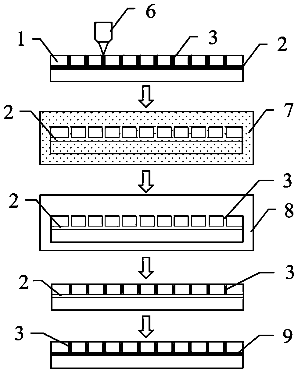
[0032] In order to make the object, technical solution and advantages of the present invention clearer, the present invention will be further described in detail below in conjunction with specific embodiments and with reference to the accompanying drawings.

[0033] The present invention proposes a method for preparing a three-dimensional optical waveguide and a photonic device structure in a transparent material by using an ultrafast laser, which includes:

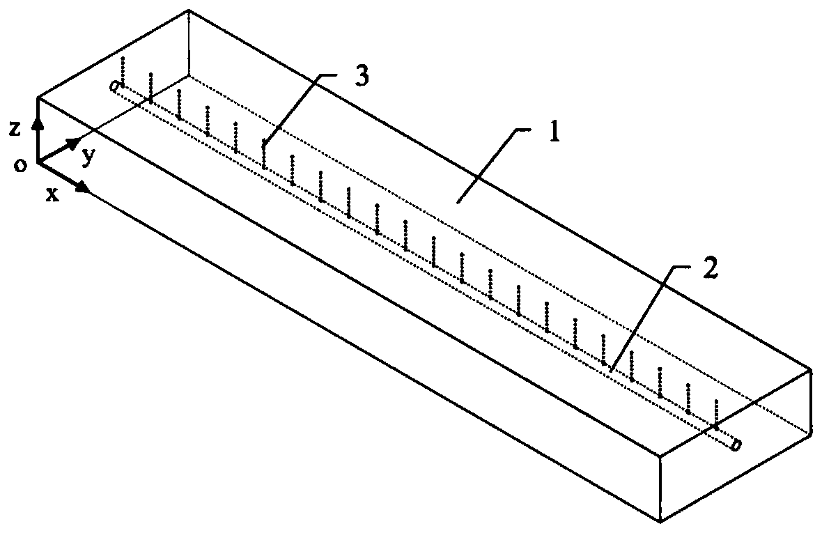
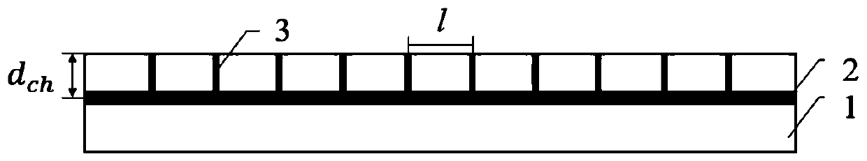
[0034] Step 1. Fix the transparent material sample on the three-dimensional movable processing platform, focus the ultrafast laser into the sample through the microscope objective lens, use the three-dimensional platform to drive the sample to move, and realize the spatial selective modification of the laser in the sample. Thus, the direct-write processing of the internal channel pattern of the sample is obtained. In order to ensure that microchannels with uniform and controllable diameters are obtained in the subsequent ...


PUM

PropertyMeasurementUnit
refractive indexaaaaaaaaaa

Abstract

The invention discloses a method for preparing a three-dimensional optical waveguide and a photonic device structure in a transparent material. The method comprises the steps of preparing a three-dimensional micro-channel in the transparent material based on the ultrafast laser selective wet etching, and then filling the micro-channel with a wave guide material, thereby forming the three-dimensional optical waveguide. Controllable preparation of various functional optical waveguide devices can be realized by manufacturing micro-channel structures with different spatial configurations. Comparedwith a traditional optical waveguide preparation method, the method has the following technical advantages that high-quality preparation of near-infrared and middle-infrared waveband waveguides, polarization-independent waveguides and active waveguide devices can be achieved by flexibly selecting filling materials, an optical waveguide mode field is flexible and controllable, and a small bendingradius can be achieved; and in combination with the three-dimensional characteristic of ultrafast laser processing, a complex three-dimensional photonic loop can be integrated on the chip in a high-density manner. Therefore, the method has important application value in the fields of optical communication networks, optical interconnection, astronomical photonics, micro-fluidic chips and the like.

Description

technical field [0001] The invention relates to the field of integrated optical waveguide preparation technology, integrated optical waveguide devices and ultrafast laser micro-nano processing, in particular to a method for preparing three-dimensional optical waveguides and photonic device structures inside transparent materials using ultrafast lasers. Background technique [0002] Optical waveguide preparation technology is a highly applicable technology. In order to realize the transmission and manipulation of light, various optical waveguide preparation technologies have been developed based on different materials. Optical waveguide devices with various characteristics can be made by using optical waveguides, and an integrated optical circuit with specific functions can be formed by integrating optical waveguides and optical waveguide devices. However, most of the optical waveguides produced by the current preparation technology are planar two-dimensional optical wavegui...

Claims


Application Information

Patent Timeline
Patent Type & Authority Applications(China)
IPC IPC(8): G02B6/00G02B6/12G02B6/13
CPCG02B6/00G02B6/12002G02B6/13G02B2006/121G02B2006/12166
Inventor 程亚刘争明徐剑
Owner EAST CHINA NORMAL UNIV
Why Eureka
Try Eureka