Array substrate and driving method thereof, display panel and display device

A technology for array substrates and drive modules, applied to static indicators, instruments, etc., can solve the problems of poor image display effects on display panels, achieve small fluctuations in size, improve image display effects, and improve flickering effects

Active Publication Date: 2020-08-04
WUHAN TIANMA MICRO ELECTRONICS CO LTD
View PDF5 Cites 32 Cited by
  • Summary
  • Abstract
  • Description
  • Claims
  • Application Information

AI Technical Summary

Problems solved by technology

At present, when the pixel circuit drives the light-emitting module to emit light, in the power-saving mode of the display panel, the flicker phenomenon is obvious, and the image display effect of the display panel is poor.

Method used


Image

  • Array substrate and driving method thereof, display panel and display device
  • Array substrate and driving method thereof, display panel and display device
  • Array substrate and driving method thereof, display panel and display device

Examples


Embodiment Construction

[0048] The present invention will be further described in detail below in conjunction with the accompanying drawings and embodiments. It should be understood that the specific embodiments described here are only used to explain the present invention, but not to limit the present invention. In addition, it should be noted that, for the convenience of description, only some structures related to the present invention are shown in the drawings but not all structures.

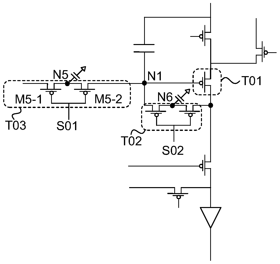
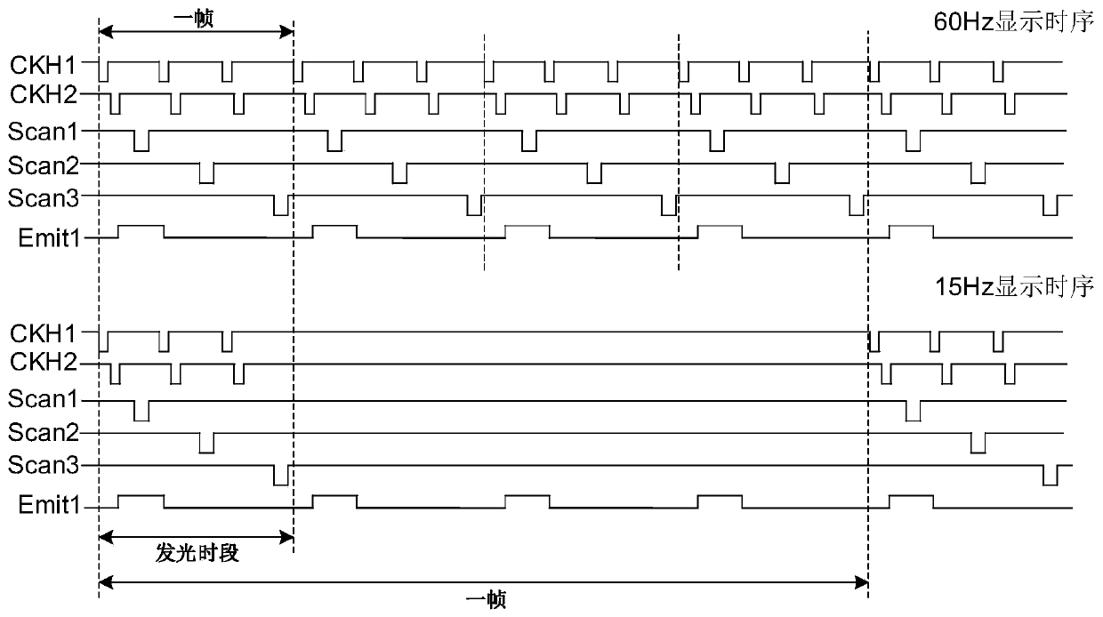
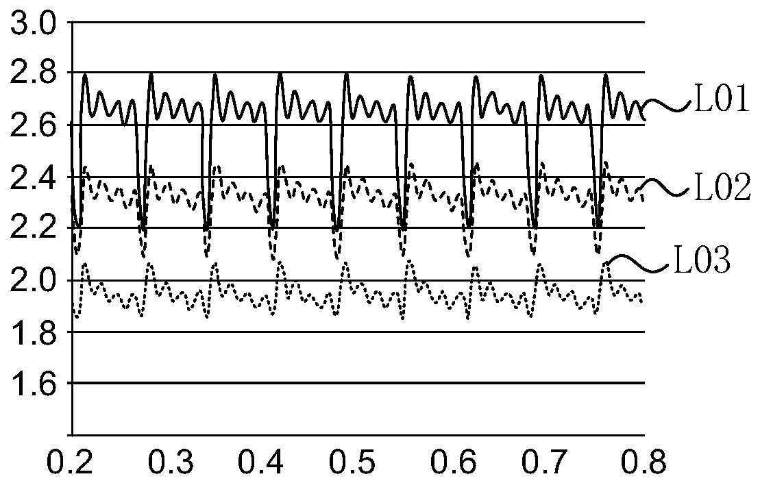
[0049] figure 1 It is a schematic structural diagram of a pixel circuit in an array substrate of the related art, figure 2 for figure 1 The driving timing diagram of the pixel circuit shown, image 3 for figure 1 The pixel circuit shown in the figure 2 The schematic diagram of the brightness change under the 15Hz display timing is shown. combine Figure 1-Figure 3 , in related technologies, adopt figure 1 shows the pixel circuit, performing figure 2The timing shown can realize image display in normal mo...


PUM


Abstract

The embodiment of the invention discloses an array substrate and a driving method thereof, a display panel and a display device. The array substrate comprises pixel circuits arranged in an array mode,wherein a first initialization module and a second initialization module are connected in series between an initialization signal end and the control end of the driving module; the output end of thesecond initialization module is electrically connected to the control end of the driving module, the output end of the first initialization module and the input end of the second initialization moduleare electrically connected to the first intermediate node, and the first pole of a light emitting module is electrically connected to a reset node; the control end of the first initialization moduleis used for receiving a first additional scanning signal, and the control end of the second initialization module is used for receiving a first scanning signal; and in at least one light-emitting period of a frame duration, the effective level end time of the first additional scanning signal lags behind the effective level end time of the first scanning signal. Therefore, the flicker phenomenon ofthe power-saving mode can be improved, and the image display effect of the display panel and the display device can be improved.

Description

technical field [0001] The present invention relates to the field of display technology, in particular to an array substrate and a driving method thereof, a display panel and a display device. Background technique [0002] With the development of display technology, active matrix organic light emitting diode (Active Matrix Organic Light Emitting Diode, AMOLED) display panel gradually entered the market, compared with traditional thin film transistor liquid crystal display panel (Thin Film Transistor Liquid Crystal Display, TFT LCD), The AMOLED display panel has the advantages of low energy consumption, self-illumination, wide viewing angle, fast response speed, and easy application to flexible display technology. The AMOLED display panel can generally be driven by current, that is, the light-emitting module is controlled to emit light by using the driving current. [0003] In order to realize the control of the driving current flowing through the light-emitting module, it i...

Claims


Application Information

Patent Timeline
Patent Type & Authority Applications(China)
IPC IPC(8): G09G3/3233G09G3/3266
CPCG09G3/3233G09G3/3266G09G2300/0814G09G2300/0866G09G2300/0819G09G3/325G09G3/3275
Inventor 张蒙蒙高娅娜周星耀曾冉冉
Owner WUHAN TIANMA MICRO ELECTRONICS CO LTD
Why Eureka
Try Eureka