Display panel, manufacturing method thereof and display device

A display panel and display area technology, applied in semiconductor/solid-state device manufacturing, instruments, acquisition/organization of fingerprints/palmprints, etc., can solve the problem of affecting the sensitivity of the fingerprint recognition unit, affecting the pixel density of the display panel, and difficult to achieve the fingerprint recognition effect. And other issues

Active Publication Date: 2020-08-07
BOE TECH GRP CO LTD +1
View PDF5 Cites 2 Cited by
  • Summary
  • Abstract
  • Description
  • Claims
  • Application Information

AI Technical Summary

Problems solved by technology

[0003] However, in the fingerprint identification panel in the prior art, the fingerprint identification unit is arranged in the gap between a plurality of pixel units in the display panel, and as the display panel develops towards high resolution, the pixel unit The gap is getting smaller and smaller....

Method used


Image

  • Display panel, manufacturing method thereof and display device
  • Display panel, manufacturing method thereof and display device
  • Display panel, manufacturing method thereof and display device

Examples


Embodiment Construction

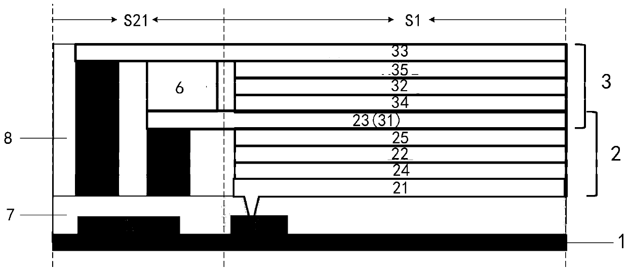
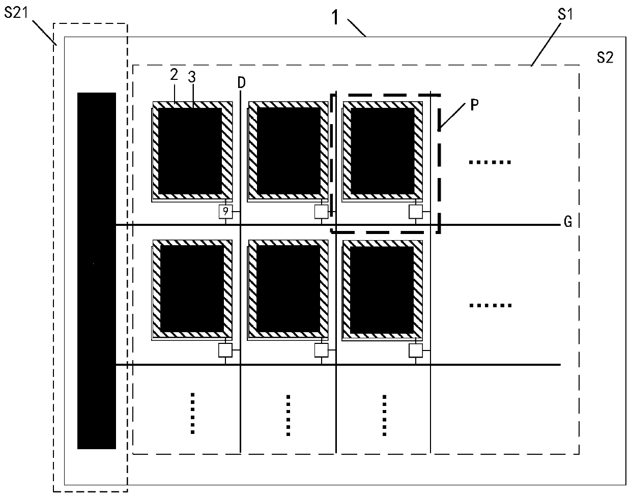
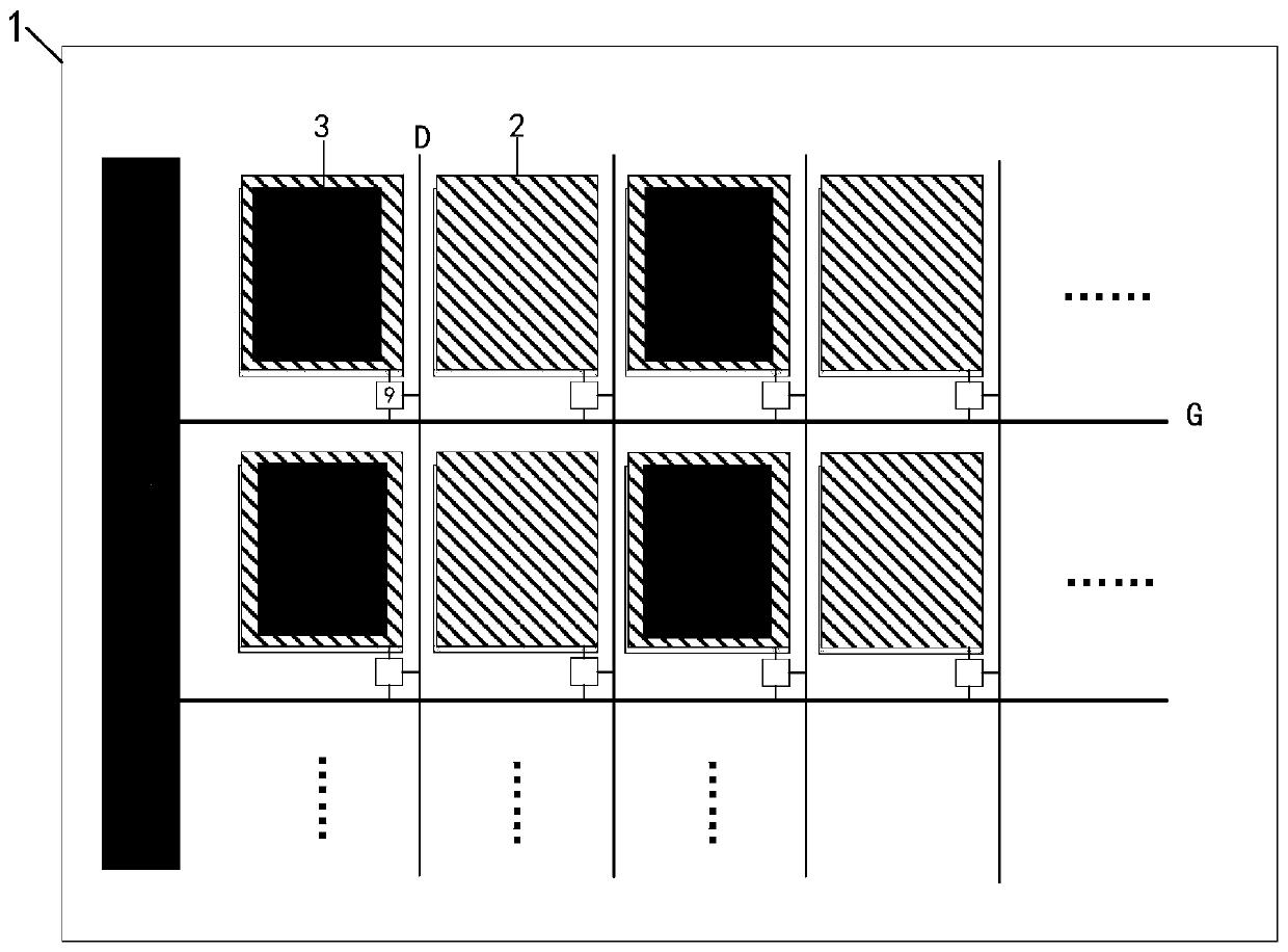
[0033] In order to make the purpose, technical solutions and advantages of the present invention clearer, the present invention will be further described in detail below in conjunction with the accompanying drawings. Obviously, the described embodiments are only some embodiments of the present invention, rather than all embodiments. Based on the embodiments of the present invention, all other embodiments obtained by persons of ordinary skill in the art without making creative efforts belong to the protection scope of the present invention.

[0034] The shapes and sizes of the components in the drawings do not reflect the actual scale, and the purpose is only to facilitate the understanding of the content of the embodiments of the present invention.

[0035] Unless otherwise defined, the technical terms or scientific terms used in the present disclosure shall have the usual meanings understood by those skilled in the art to which the present disclosure belongs. "First", "second...


PUM


Abstract

The invention provides a display panel, a manufacturing method thereof and a display device, whichbelong to the technical field of display. The display panel comprises a substrate, a plurality of light emitting devices and a plurality of fingerprint identification units,wherein the plurality of light-emitting devices are arranged at one side of the substrate, the plurality of fingerprint identification units are arranged at one side, deviating from the substrate, of the lightemitting device located in the fingerprint identification area, and at least one fingerprint identification unit and onelightemitting device located in the fingerprint identification area are arranged in a stacked mode. The fingerprint identification unit in the display panel provided by the invention does not need tooccupy extra space of the layer where the lightemitting device is located, so that the fingerprint identification unit can be prevented from influencing the resolution of the display panel, and the fingerprint identification unit can be prevented from influencing the lightemitting rate of the lightemitting device.

Description

technical field [0001] The invention belongs to the field of display technology, and in particular relates to a display panel, a manufacturing method thereof, and a display device. Background technique [0002] With the development of display technology, the display panel with fingerprint identification function has become the mainstream. Usually, a fingerprint identification unit is arranged in the fingerprint identification area of ​​the display panel, and fingerprint identification is realized according to the change of the light intensity received by the fingerprint identification unit. [0003] However, in the fingerprint identification panel in the prior art, the fingerprint identification unit is arranged in the gap between a plurality of pixel units in the display panel, and as the display panel develops towards high resolution, the pixel unit The gap is getting smaller and smaller. If the fingerprint recognition unit is set in the gap, it will affect the pixel densi...

Claims


Application Information

Patent Timeline
IPC IPC(8): H01L27/32H01L21/77G06K9/00
CPCG06V40/1318H10K59/60H10K59/12H10K59/1201
Inventor 陈友春赖韦霖鲍建东王文强
Owner BOE TECH GRP CO LTD
Why Eureka
Try Eureka