A kind of sputtering method of semiconductor chip

A semiconductor and chip technology, which is applied in the field of sputtering of semiconductor chips, can solve problems such as troublesome processing, irregular shapes, and complicated processes, and achieve the effects of reducing costs, conveniently separating and tearing glue, and conveniently clamping and taking out

Active Publication Date: 2021-11-16
HIMIT (SHENZHEN) TECH CO LTD
View PDF0 Cites 0 Cited by
  • Summary
  • Abstract
  • Description
  • Claims
  • Application Information

AI Technical Summary

Problems solved by technology

[0002] For the sputtering process of semiconductor chips, the existing technology is generally only suitable for conventional semiconductor chips. The shape of the semiconductor chip is regular, and the shape of the sputtering area is usually a whole surface. Rules, the same side has both sputtering area and non-sputtering area (protection area) that needs to be protected. The existing technology cannot handle semiconductor chips with special shapes and selective area sputtering. Complex, troublesome processing, high NG rate

Method used


Image

  • A kind of sputtering method of semiconductor chip
  • A kind of sputtering method of semiconductor chip
  • A kind of sputtering method of semiconductor chip

Examples


Embodiment 1

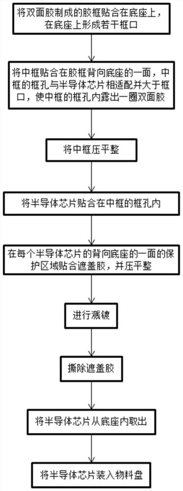
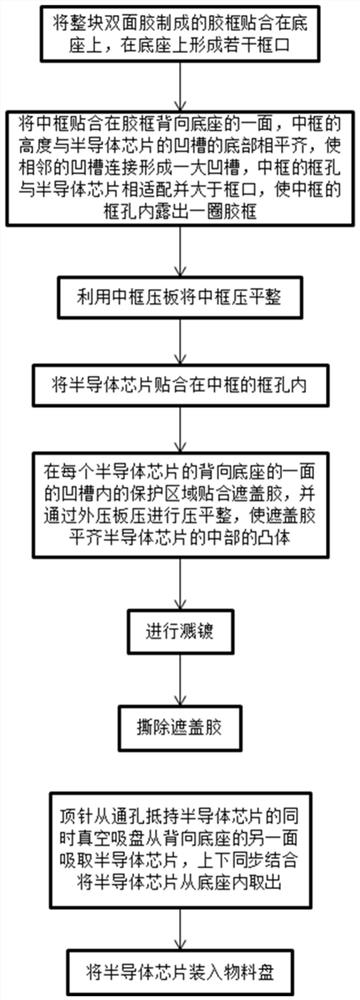
[0061] See Figure 1-Figure 8 ,

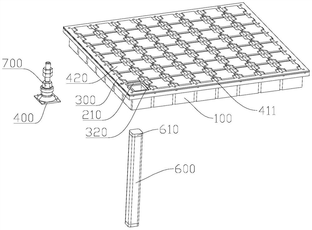
[0062] A. Lay the plastic frame 200 made of a whole piece of double-sided adhesive on the base 100, and form a number of frame openings 210 on the base 100; the base 100 is provided with a number of through holes 110 in an array, and the through holes 110 are criss-crossed A plurality of exhaust grooves 120 are provided, and a first air hole 130 is provided at the intersection of the exhaust grooves 120; Two air holes 220;

[0063] B. Attach the middle frame 300 on the side of the plastic frame 200 facing away from the base 100, the height of the middle frame 300 is flush with the bottom of the groove 410 of the semiconductor chip 400, so that the adjacent grooves 410 are connected to form a large concave Groove 411, the frame hole 310 of the middle frame 300 is adapted to the semiconductor chip 400 and is larger than the frame opening 210, so that a circle of plastic frame 200 is exposed in the frame hole 310 of the middle frame 300; the mi...


PUM


Abstract

The invention relates to a semiconductor chip sputtering method, especially for semiconductor chips with irregular shapes and sputtering in selective areas, the semiconductor chip is fixed through the cooperation of the base, the plastic frame and the middle frame, and the protection area is covered by the covering glue , can protect the non-sputtering area and avoid NG products; the middle frame can prevent the rubber frame from being too tightly connected with the covering glue, which will cause inconvenience in taking out, and it is convenient to separate and tear the glue, and it is convenient to glue the whole piece of double-sided adhesive at one time. The frame is removed from the base, which can also facilitate the clamping and removal of the semiconductor chip, isolate the non-sputtering area on the side of the semiconductor chip, and reduce the cost. The middle frame can be replaced according to different types and shapes of semiconductor chips.

Description

technical field [0001] The invention relates to the technical field of semiconductor chip sputtering, in particular to a semiconductor chip sputtering method. Background technique [0002] For the sputtering process of semiconductor chips, the existing technology is generally only suitable for conventional semiconductor chips. The shape of the semiconductor chip is regular, and the shape of the sputtering area is usually a whole surface. Rules, the same side has both sputtering area and non-sputtering area (protection area) that needs to be protected. The existing technology cannot handle semiconductor chips with special shapes and selective area sputtering. Complex, troublesome processing, high NG rate. Contents of the invention [0003] In view of the above situation, it is necessary to provide a sputtering method suitable for semiconductor chips with irregular shapes and requiring selective area sputtering. [0004] In order to solve the above technical problems, the ...

Claims


Application Information

Patent Timeline
Patent Type & Authority Patents(China)
IPC IPC(8): C23C14/34C23C14/04H01L21/673
CPCC23C14/042C23C14/34H01L21/67333
Inventor 蒋海兵
Owner HIMIT (SHENZHEN) TECH CO LTD
Why Eureka
Try Eureka