Display panel and display device

A display panel and display area technology, applied in semiconductor devices, electrical components, circuits, etc., can solve the problems of signal transmission delay and affect display uniformity, and achieve the effect of reducing delay, improving display uniformity, and reducing equivalent resistance

Pending Publication Date: 2020-08-25
BOE TECH GRP CO LTD +1
View PDF2 Cites 12 Cited by
  • Summary
  • Abstract
  • Description
  • Claims
  • Application Information

AI Technical Summary

Problems solved by technology

However, as the size of the OLED display panel increases, the loading (load) of the signal line transmitting the signal in the OLED display panel increases, resulting in a delay in signal transmission, which in turn affects display uniformity.

Method used


Image

  • Display panel and display device
  • Display panel and display device
  • Display panel and display device

Examples


Embodiment Construction

[0037] In order to make the object, technical solution and advantages of the present invention more clear, the specific implementation manners of the display panel and the display device provided by the embodiments of the present invention will be described in detail below with reference to the accompanying drawings. It should be understood that the preferred embodiments described below are only used to illustrate and explain the present invention, not to limit the present invention. And in the case of no conflict, the embodiments in the present application and the features in the embodiments can be combined with each other.

[0038] The thickness, size and shape of each layer of film in the drawings do not reflect the real proportion of the display panel, but are only intended to schematically illustrate the content of the present invention.

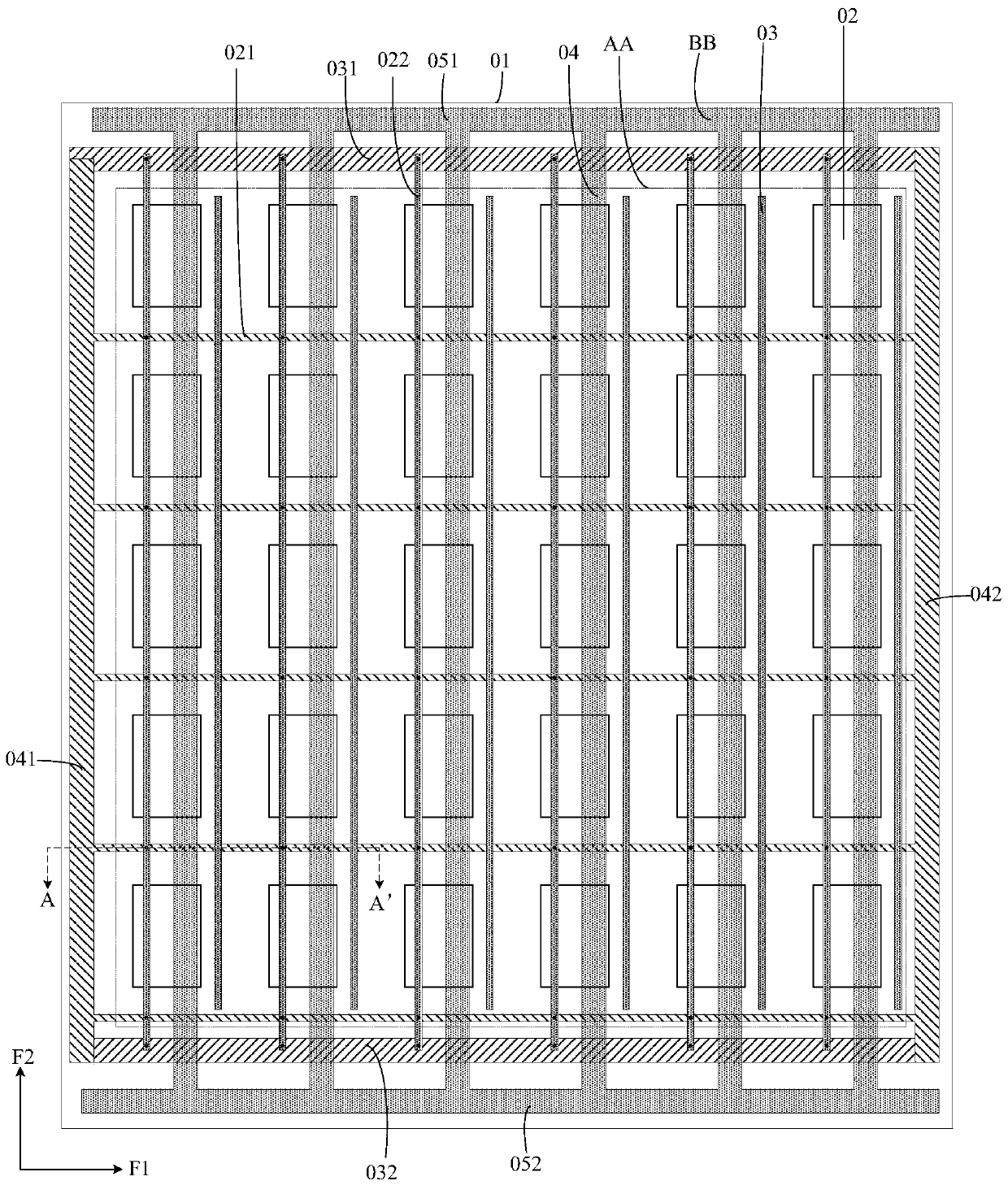
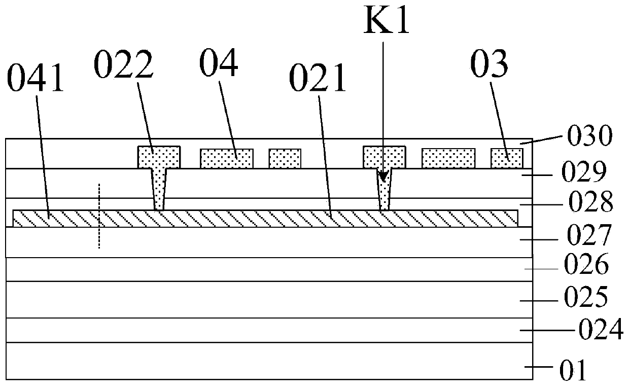
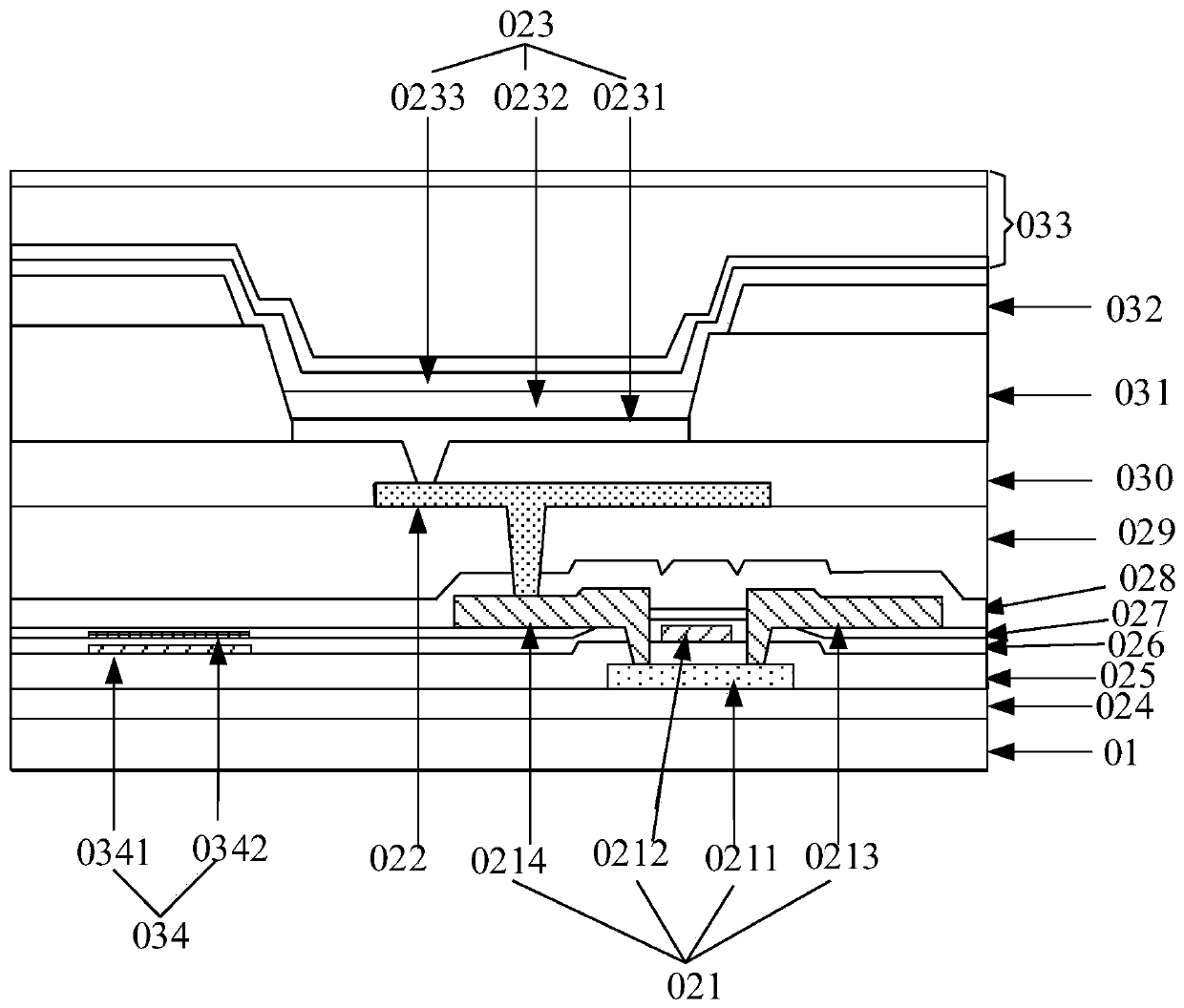
[0039] The display panel provided by the embodiment of the present invention, such as figure 1 As shown, it includes: a base substrat...


PUM


Abstract

The invention discloses a display panel and a display device. An auxiliary signal line crossed with an initialization signal line is arranged; a first via hole is formed in the intersection of the initialization signal line and the auxiliary signal line; the corresponding initialization signal lines and the auxiliary signal lines are electrically connected through the first via holes, so that theinitialization signal lines and the auxiliary signal lines which are electrically connected are connected in parallel, equivalently, the initialization signal lines are connected with a resistor in parallel; and therefore the equivalent resistance of the initialization signal lines can be reduced. Due to the fact that the larger the length of the initialization signal lines is, the larger the number of the first via holes corresponding to the initialization signal lines is, the larger the length of the initialization signal lines is, the more the resistors connected with the initialization signal lines in parallel are, delay of signal transmission can be reduced. The display panel can be easily applied to a large-size display device, and the display uniformity is improved.

Description

technical field [0001] The invention relates to the field of display technology, in particular to a display panel and a display device. Background technique [0002] The organic light-emitting diode (Organic Light-Emitting Diode, OLED) display panel is one of the hotspots in the field of flat panel display research. With the development of display technology, OLED display panels are gradually developing towards large and medium sizes. However, as the size of the OLED display panel increases, the loading (load) of the signal line transmitting the signal in the OLED display panel increases, thereby causing a delay in signal transmission, thereby affecting display uniformity. Contents of the invention [0003] Embodiments of the present invention provide a display panel and a display device for improving display uniformity of the display panel. [0004] An embodiment of the present invention provides a display panel, including: [0005] a substrate substrate having a displ...

Claims


Application Information

Patent Timeline
Patent Type & Authority Applications(China)
IPC IPC(8): H01L27/32
CPCH10K59/12H10K59/131H01L27/124H10K59/1315H01L27/1255H10K59/1213H10K59/1216
Inventor 杨中流陈文波樊萌月张兵赵爽杨静陈祯祐
Owner BOE TECH GRP CO LTD
Why Eureka
Try Eureka