Reverse connection prevention circuit
An anti-reverse circuit and interface technology, applied in emergency protection circuit devices, electrical components, etc., can solve problems such as small practical application range
- Summary
- Abstract
- Description
- Claims
- Application Information
AI Technical Summary
Problems solved by technology
Method used
Image

Examples
Embodiment 1
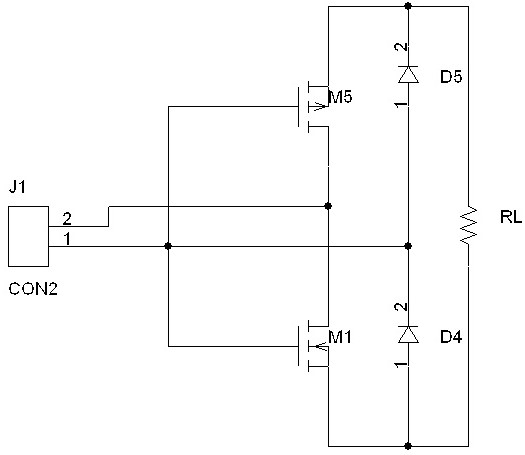
[0023] to combine figure 1 , an anti-reverse connection circuit, the anti-reverse connection circuit is connected to an external interface J1 composed of a first pin and a second pin, and is characterized in that the anti-reverse connection circuit includes an NMOS transistor M1 and a PMOS transistor M5, a first diode tube D4 and the second diode D5, where:
[0024] - the cathode of the first diode D4, the anode of the second diode D5, the gate of the NMOS transistor M1, and the gate of the PMOS transistor M5 are all connected to the first pin of the external interface J1;
[0025] - the drain of the NMOS transistor M1 and the drain of the PMOS transistor M5 are both connected to the second pin of the external interface J1;
[0026] - the source of the NMOS transistor M1 is connected to the anode of the first diode D4, and the source of the PMOS transistor M5 is connected to the cathode of the second diode D5;
[0027] - Both ends of the load RL are respectively connected to...
Embodiment 2
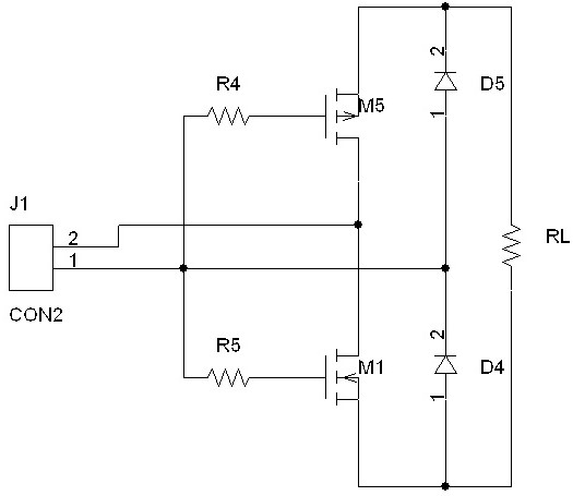
[0033] to combine figure 2 The difference between this embodiment and Embodiment 1 is that it also includes a first current limiting resistor R4 and a second current limiting resistor R5, the gate of the PMOS transistor M5 is connected to the external interface J1 through the first current limiting resistor R4 The first pin of the NMOS transistor M1 is connected to the first pin of the external interface J1 through the second current limiting resistor R5.
[0034] The protection resistor can be used to adjust the on-off speed of the MOS tube. When the gate protection resistance is small, the on-off speed of the MOS tube is fast and the switching loss is small; on the contrary, when the gate protection resistance is large, the on-off speed of the MOS tube is slow. Switching losses are high. However, if the on-off speed is too fast, the voltage and current change rate of the MOS tube will be greatly increased, thereby generating greater interference and affecting the work of t...
Embodiment 3
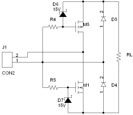
[0036] to combine image 3 , The difference between this embodiment and Embodiment 2 is that it includes both the first zener diode D6 and the second zener diode D7, and the first current limiting resistor R4 and the second current limiting resistor R5; the first zener diode D6 Connected between the gate and the source of the PMOS transistor M5; the second Zener diode D7 is connected between the gate and the source of the NMOS transistor M1. The gate of the PMOS transistor M5 is connected to the first pin of the external interface J1 through the first current limiting resistor R4; the gate of the NMOS transistor M1 is connected to the first pin of the external interface J1 through the second current limiting resistor R5. a pin.
[0037] This scheme has all advantages of embodiment 1-2 concurrently.
[0038] At the same time, when the input voltage is higher than the highest voltage of the gate of the MOS transistor, the Zener diode connected to the gate and the source can pr...
PUM
 Abstract
Description
Claims
Application Information
 - R&D
- Intellectual Property
- Life Sciences
- Materials
- Tech Scout
- Unparalleled Data Quality
- Higher Quality Content
- 60% Fewer Hallucinations
Browse by: Latest US Patents, China's latest patents, Technical Efficacy Thesaurus, Application Domain, Technology Topic, Popular Technical Reports.
© 2025 PatSnap. All rights reserved.Legal|Privacy policy|Modern Slavery Act Transparency Statement|Sitemap|About US| Contact US: help@patsnap.com