Silicon wafer carrier plate, carrier plate electrode device and coating equipment
A technology of electrode device and carrier plate, applied in gaseous chemical plating, metal material coating process, coating, etc., can solve the problems affecting the coating effect of silicon wafers, uneven electric field, etc.
- Summary
- Abstract
- Description
- Claims
- Application Information
AI Technical Summary
Problems solved by technology
Method used
Image

Examples
Embodiment 1
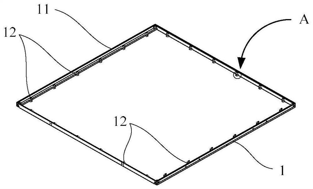
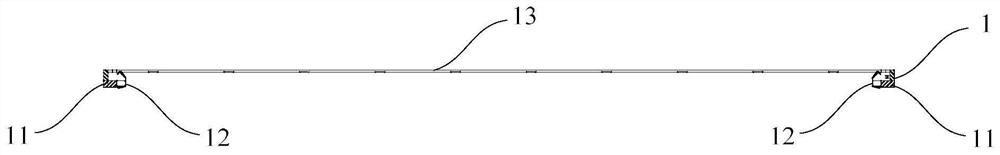
[0052] In this embodiment, a silicon wafer carrier 1 is provided. Such as figure 1 and figure 2 As shown, the silicon wafer carrier 1 includes a carrier frame 11 , a plurality of first electrode assemblies 12 and a tray 13 .
[0053] The carrier frame 11 serves as a mounting base for the first electrode assembly 12 and the tray 13 . A plurality of first electrode assemblies 12 are arranged at intervals on the inner side of the carrier frame 11 along the circumferential direction of the carrier frame 11, and the tray 13 is arranged on the top of the plurality of first electrode assemblies 12, and the silicon wafer is carried by the tray 13 to realize silicon The wafer moves with the silicon wafer carrier 1 so as to enter the coating process cavity 21 for coating process. Wherein, the first electrode assembly 12 extends to the bottom of the carrier frame 11, so that when the silicon chip carrier 1 enters the coating process chamber 21 as a whole, the bottom of the first elec...
Embodiment 2
[0056] In this embodiment, a silicon wafer carrier 1 is provided, which is further improved on the basis of the first embodiment.
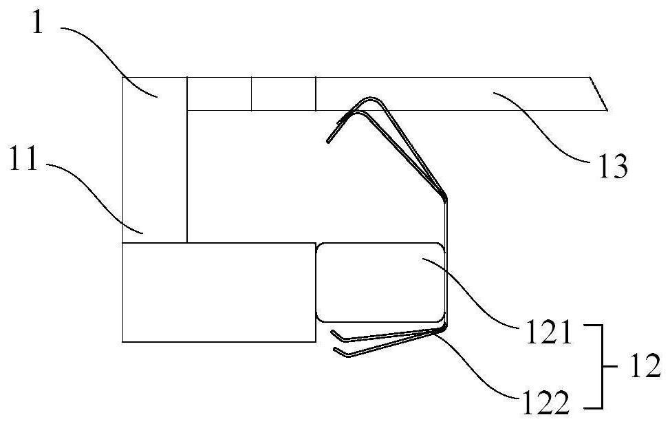
[0057] Such as Figure 2 to Figure 4 As shown, the first electrode assembly 12 includes a fixing block 121 and a first electrode sheet 122 . The fixing block 121 is connected to the inner side of the carrier frame 11 , and the first electrode sheet 122 is connected to an end of the fixing block 121 away from the carrier frame 11 , so as to realize the installation and fixing of the first electrode sheet 122 . The top of the first electrode sheet 122 stretches out to the top of the fixed block 121, to support the tray 13 by the top of the first electrode sheet 122; When the silicon chip carrier 1 enters the coating process cavity 21, the bottom of the first electrode sheet 122 contacts the supporting structure of the coating process cavity 21, so that the silicon wafer placed on the tray 13 can pass through The tray 13 and the first electrode she...
Embodiment 3
[0061] This embodiment provides a silicon chip carrier 1, which is further improved on the basis of the second embodiment.
[0062] Such as Figure 5 and Figure 6As shown, the carrier frame 11 further includes at least one support rod 14 and a plurality of second electrode sheets 15 . The supporting rods 14 are arranged in the carrier frame 11, and the two ends of the supporting rods 14 are connected with the carrier frame 11, so that the carrier frame 11 and the supporting rods 14 form a plurality of frame-shaped structures, forming a grid-like structure as a whole , so that a tray 13 is correspondingly provided in each frame structure. Wherein, the number of support rods 14 can be specifically set according to the shape and size of the carrier frame 11 and the tray 13 . When the number of support rods 14 is multiple, the multiple support rods 14 can be arranged sequentially in the same direction, or can be arranged crosswise.
[0063] A plurality of second electrode she...
PUM
 Abstract
Description
Claims
Application Information
 - R&D Engineer
- R&D Manager
- IP Professional
- Industry Leading Data Capabilities
- Powerful AI technology
- Patent DNA Extraction
Browse by: Latest US Patents, China's latest patents, Technical Efficacy Thesaurus, Application Domain, Technology Topic.
© 2024 PatSnap. All rights reserved.Legal|Privacy policy|Modern Slavery Act Transparency Statement|Sitemap