
Eureka
For R&D, Eureka makes reading and utilizing patents & technical documents easy.
Eureka AIR
Designed for self-driven R&D workflows. Generate viable solutions, solve complex R&D challenges, empower your innovation with AI.

Eureka Materials
Designed for material experts only. Revolutionize your material R&D, from search, analyze, to developing new materials.

TechResearch
Generate reliable direction feasibility study reports for your R&D in just a few steps.

TechSeek
Discover and master advanced knowledge NOW. Basics, ideas, possibilities, all at once.

TechMind
As an expert in R&D Theories, TechMind can generates customized viable solutions instantly.

TechRisk
Analyze your overall solution with one click, know your potential R&D risks in advance.

TechMonitor
Get weekly tech updates, stay abreast of the latest tech innovations and key insights.
Temporary bonding method
A temporary bonding and debonding technology, used in electrical components, semiconductor/solid-state device manufacturing, circuits, etc., can solve the problems of high material cost, high stress, long debonding time, etc., to promote development, save material costs, and reduce debonding. effect of time
- Summary
- Abstract
- Description
- Claims
- Application Information
AI Technical Summary
Problems solved by technology
Method used
Image

Examples
Embodiment Construction
[0019] Specific embodiments of the present disclosure will be described in detail below in conjunction with the accompanying drawings. It should be understood that the specific embodiments described here are only used to illustrate and explain the present disclosure, and are not intended to limit the present disclosure.
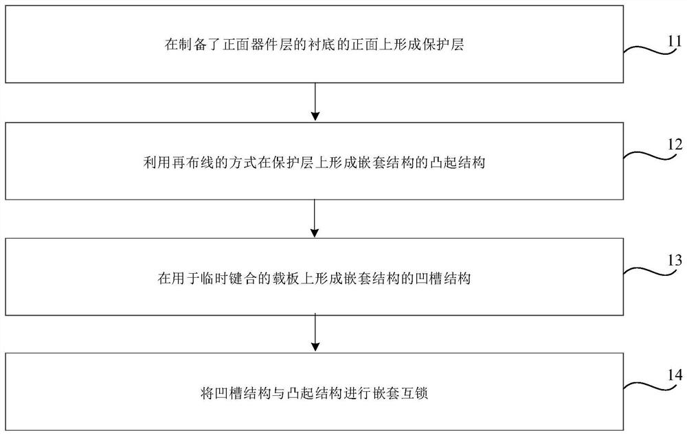
[0020] figure 1 is a flowchart of a temporary bonding method according to an embodiment of the present disclosure. Such as figure 1 As shown, the method includes the following steps S11 to S14.
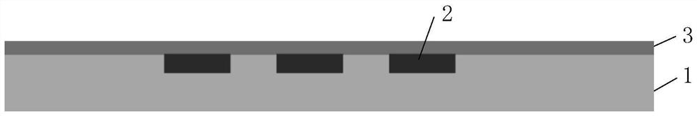
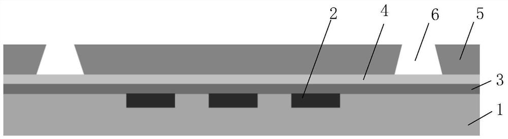
[0021] In step S11, a protective layer is formed on the front surface of the substrate on which the front device layer is prepared.
[0022] The protection layer is mainly used to protect the front device layer in subsequent steps to prevent the front device layer from being damaged.
[0023] The material of the protective layer may be silicon dioxide, silicon nitride, polyimide, phenylpropene cyclobutene and the like. The thickness of the protective layer may b...
PUM
| Property | Measurement | Unit |
|---|---|---|
| thickness | aaaaa | aaaaa |
Abstract
Description
Claims
Application Information
 - R&D Engineer
- R&D Manager
- IP Professional
- Industry Leading Data Capabilities
- Powerful AI technology
- Patent DNA Extraction
Browse by: Latest US Patents, China's latest patents, Technical Efficacy Thesaurus, Application Domain, Technology Topic, Popular Technical Reports.
© 2024 PatSnap. All rights reserved.Legal|Privacy policy|Modern Slavery Act Transparency Statement|Sitemap|About US| Contact US: help@patsnap.com