Supercharge Your Innovation With Domain-Expert AI Agents!

Circuit board negative film and processing method thereof

A processing method and circuit board technology, applied in the directions of printed circuits, printed circuit manufacturing, and mechanically removing conductive materials, can solve problems such as deformation, slot burrs, etc., achieve excellent performance, prevent damage to the board, and simple design reasonable effect

Active Publication Date: 2021-04-06
广东世运电路科技股份有限公司
View PDF28 Cites 0 Cited by
  • Summary
  • Abstract
  • Description
  • Claims
  • Application Information

AI Technical Summary

Problems solved by technology

[0004] In order to solve the above problems, the object of the present invention is to provide a circuit board negative and its processing method, which can effectively solve the problems of burrs and deformation in slot holes

Method used


Image

  • Circuit board negative film and processing method thereof
  • Circuit board negative film and processing method thereof
  • Circuit board negative film and processing method thereof

Examples


Embodiment Construction

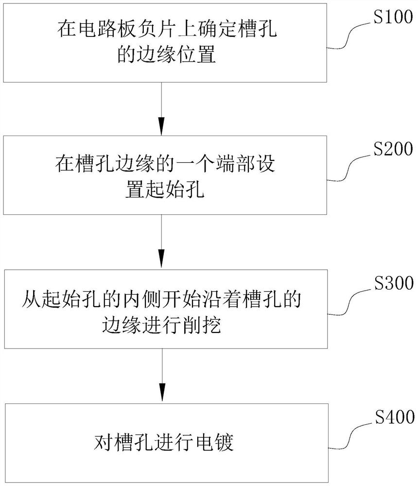
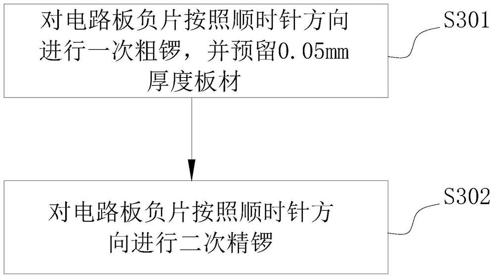
[0025] This part will describe the specific embodiment of the present invention in detail, and the preferred embodiment of the present invention is shown in the accompanying drawings. Each technical feature and overall technical solution of the invention, but it should not be understood as a limitation on the protection scope of the present invention.

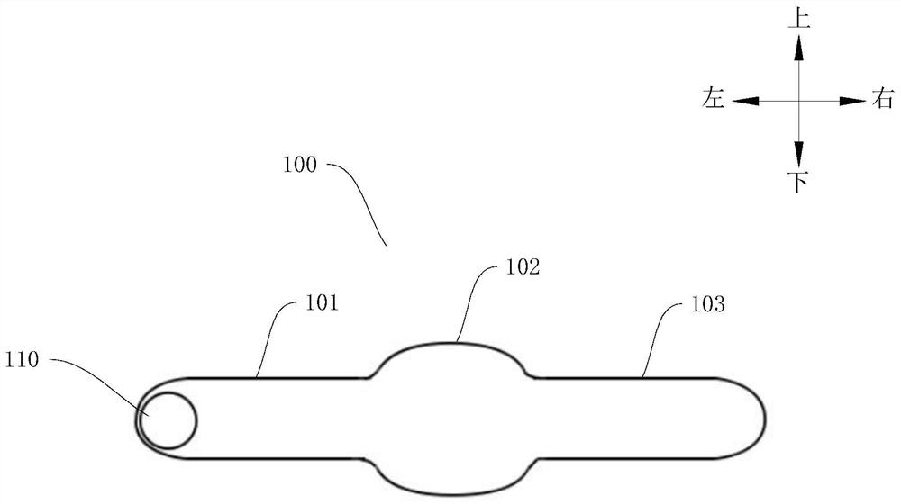
[0026] In the description of the present invention, it should be understood that the orientation descriptions, such as up, down, front, back, left, right, etc. indicated orientations or positional relationships are based on the orientations or positional relationships shown in the drawings, and are only In order to facilitate the description of the present invention and simplify the description, it does not indicate or imply that the device or element referred to must have a specific orientation, be constructed and operated in a specific orientation, and thus should not be construed as limiting the present invention.

[0027] I...


PUM


Abstract

The invention discloses a circuit board negative film and a processing method thereof. The circuit board negative film is provided with a slotted hole, the slotted hole comprises a first part, a second part and a third part, the second part is connected between the first part and the third part, the left side of the first part is an arc curved surface, and the upper and lower surfaces of the first part are parallel surfaces; the upper surface and the lower surface of the second part are both arc curved surfaces, the third part and the first part are symmetrical about the second part, rough milling and fine milling are conducted on the circuit board negative film in the clockwise direction through a milling cutter, and the problems of burrs and deformation of slotted holes are effectively solved.

Description

technical field [0001] The invention relates to the field of circuit board production, in particular to a circuit board negative and a processing method thereof. Background technique [0002] There are many large and small holes on the circuit board. Pick it up and look at the electric light on the ceiling, and you will find many densely packed small holes. These holes are not placed where to look good. Each hole has its own designed for the purpose. These holes can be roughly divided into two types: PTH (Plating Through Hole, plating through hole) and NPTH (NonPlating Through Hole, non-plating through hole). On the other hand, in addition to through holes, there are other holes in the circuit board that do not penetrate the circuit board. [0003] In the process of PCB board production, it is necessary to set slot holes on the negative of the circuit board. The current plan is: ①Drill the burr holes→②Drill the slot holes at both ends→③Drill the middle round hole. During t...

Claims


Application Information

Patent Timeline
Patent Type & Authority Applications(China)
IPC IPC(8): H05K3/00H05K3/04
CPCH05K3/0047H05K3/04
Inventor 管宏科
Owner 广东世运电路科技股份有限公司
Features
  • R&D
  • Intellectual Property
  • Life Sciences
  • Materials
  • Tech Scout
  • Unparalleled Data Quality
  • Higher Quality Content
  • 60% Fewer Hallucinations
Learn More