A transfer device and transfer method

A technology of transfer device and transfer method, which is applied in the direction of semiconductor devices, electrical components, circuits, etc., and can solve the problems of complicated operation of the transfer device

Active Publication Date: 2022-05-31
CHONGQING KONKA PHOTOELECTRIC TECH RES INST CO LTD
View PDF9 Cites 0 Cited by
  • Summary
  • Abstract
  • Description
  • Claims
  • Application Information

AI Technical Summary

Problems solved by technology

[0004] In view of the deficiencies in the prior art above, the purpose of the present invention is to provide a transfer device and a transfer method, aiming to solve the technical problem of complex operation of the existing transfer device

Method used


Image

  • A transfer device and transfer method
  • A transfer device and transfer method
  • A transfer device and transfer method

Examples


Embodiment Construction

[0032] In order to facilitate understanding of the present invention, the present invention will be described more fully hereinafter with reference to the related drawings. The preferred embodiments of the invention are shown in the accompanying drawings. However, the present invention may be embodied in many different forms and is not limited to the embodiments described herein. Rather, these embodiments are provided so that a thorough and complete understanding of the present disclosure is provided.

[0033] Unless otherwise defined, all technical and scientific terms used herein have the same meaning as commonly understood by one of ordinary skill in the art to which this invention belongs. The terms used herein in the description of the present invention are for the purpose of describing specific embodiments only, and are not intended to limit the present invention.

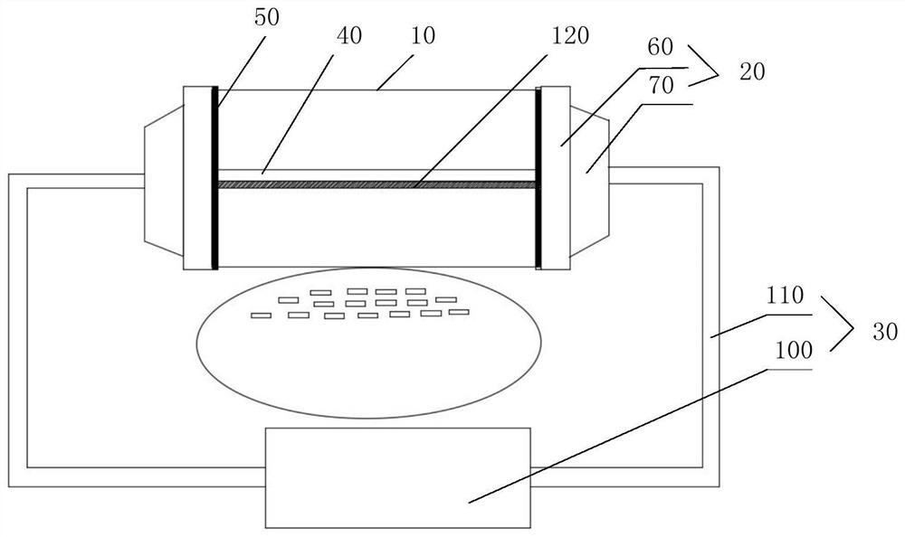
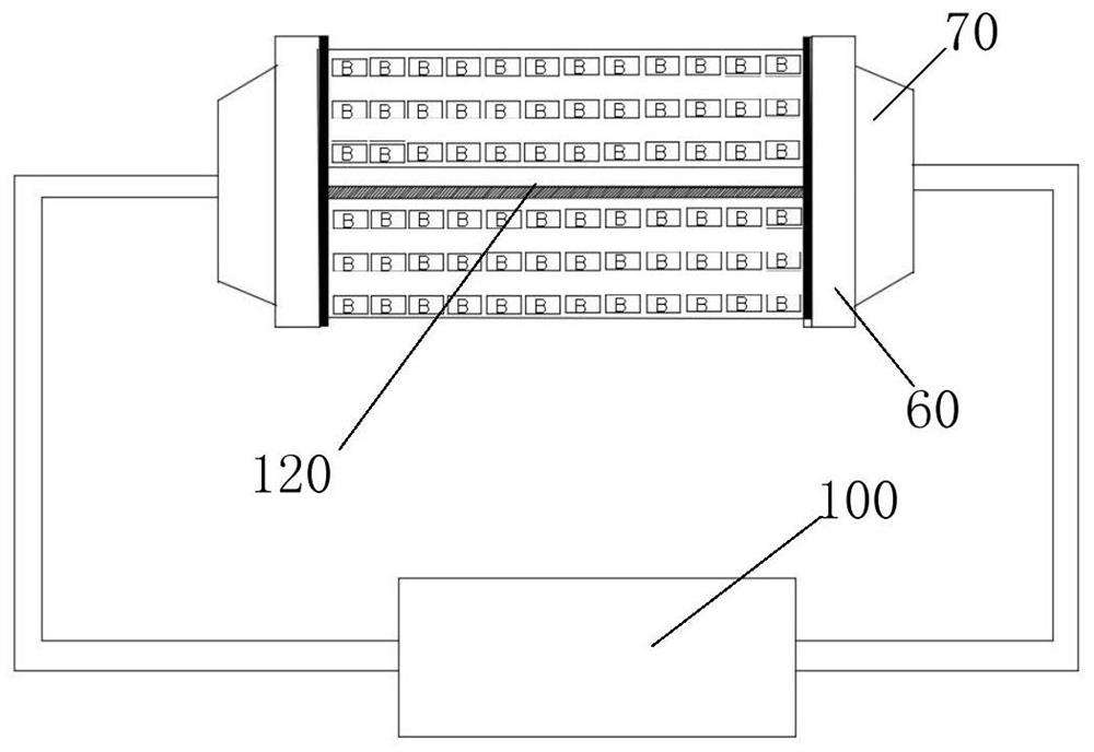
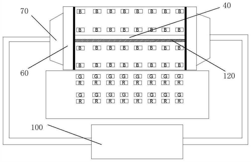
[0034] see figure 1 , a transfer device provided by the present invention, comprising:

[0035] a roll...


PUM


Abstract

The present invention provides a transfer device and a transfer method, wherein the transfer device includes a roller made of an elastic film; two rotating parts respectively arranged at both ends of the roller for driving the rotation of the roller; An air-inflating unit communicating with the roller for inflating the inside of the stretched roller; two ends respectively connected to the two rotating parts for pushing the rotating parts to radially stretch the roller a telescopic rod, and an annular clamping piece sleeved on the end of the drum for axially stretching the end of the drum. The transfer device of the present invention uses a roller made of an elastic film to transfer the micro light-emitting device. The elastic film is extensible, and the roller is stretched by the telescopic rod and the ring clamp, so that different crystal expansion distances can be realized on the roller. , The crystal expansion process is simple and easy to operate.

Description

technical field [0001] The present invention relates to the technical field of semiconductor display, and in particular, to a transfer device and a transfer method. Background technique [0002] Micro-LED (Micro Light Emitting Diode, Micro Light Emitting Diode) technology is a new generation of display technology, of which mass transfer technology is an important part of Micro-LED manufacturing. For the technology of transferring individual Micro-LEDs from a carrier substrate to a target substrate, the primary problem to be solved by mass transfer is to change the spacing between Micro-LEDs from the spacing on the carrier substrate to the spacing on the target substrate. However, the methods for mass transfer in the prior art, such as complicated operation and high cost, are not conducive to the development of Micro-LED technology. [0003] Therefore, the existing technology still needs to be improved and developed. SUMMARY OF THE INVENTION [0004] In view of the above-...

Claims


Application Information

Patent Timeline
Patent Type & Authority Patents(China)
IPC IPC(8): H01L21/683H01L33/48
CPCH01L21/6836H01L33/48H01L2221/68386H01L2221/68363H01L2933/0033
Inventor 李强许时渊
Owner CHONGQING KONKA PHOTOELECTRIC TECH RES INST CO LTD
Why Eureka
Try Eureka