Chip package
A chip packaging and chip technology, applied in measurement devices, instruments, measuring magnetic variables, etc., can solve the problems of reduced performance of current detection devices, difficult configuration of magnetic field sensors, and high through-hole resistance.
- Summary
- Abstract
- Description
- Claims
- Application Information
AI Technical Summary
Problems solved by technology
Method used
Image
Examples
no. 1 Embodiment approach >
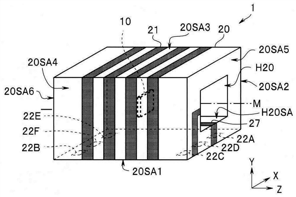
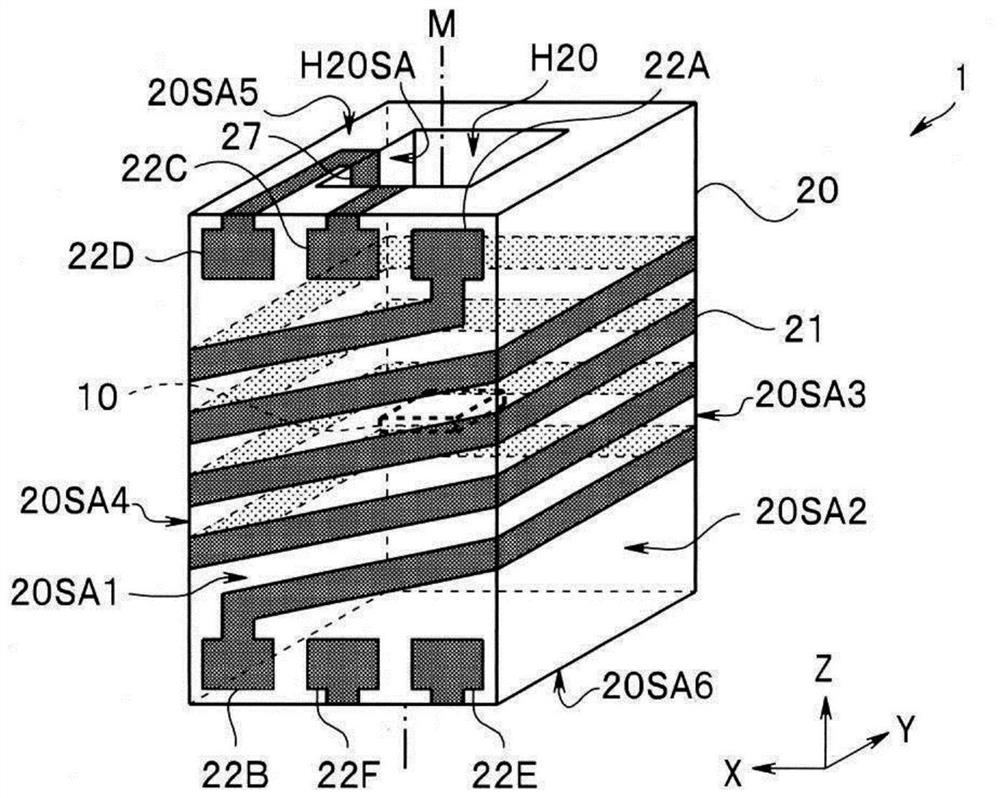
[0018] Hereinafter, the chip package 1 of the first embodiment will be described in detail with reference to the drawings.
[0019] In addition, the drawings based on the embodiment are schematic drawings, and the relationship between the thickness and width of each part, the thickness ratio of each part, the relative angle, and the like are different from actual ones. Parts in which mutual dimensional relationships and ratios are different are also included among the drawings. In addition, the illustrations and reference signs of some constituent elements are omitted.
[0020] The chip package 1 is a current detection device that detects a current. The chip package 1 is used, for example, in a high-frequency switching power supply such as a PFC power supply, an AC / DC adapter, an inverter, a control device for a motor transmission device, or a power module, but the application is not limited to these.
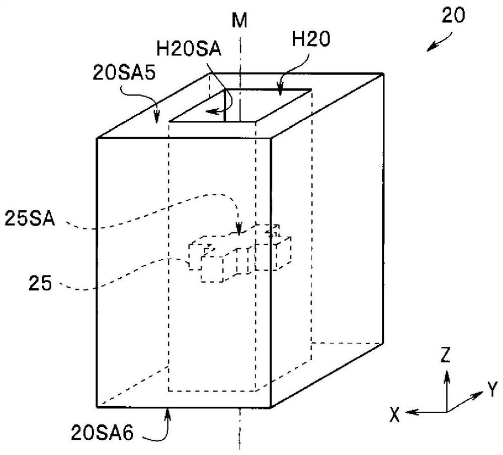
[0021] Such as figure 1 with figure 2 As shown, the chip package 1 ha...
no. 2 Embodiment approach >
[0046]The chip package 1A of this embodiment is similar to the chip package 1 . Therefore, the same reference numerals are assigned to the same function components, and the description thereof will be omitted.
[0047] exist Figure 7 In the shown chip package 1A, the mounting surface of the chip case 20A on which the first electrode pads 22A, 22B and the second electrode pads 22C to 22F are arranged is the four surfaces on which the solenoid coil 21 is wound. Outer surfaces 20SA1 to 20SA4 are perpendicular to outer surface 20SA5 . The first electrode pad 22B is connected to the solenoid coil 21 through the wiring 27 on the wall surface of the hole H20 . Wiring may also be provided on the outer surface of the chip case 20A.
[0048] Like the chip package 1 , since the chip package 1A has all the electrode pads 22A to 22F for external connection arranged on any one of its outer surfaces, it can be surface-mounted on a wiring board. In addition, the number of electrode pads ...
no. 3 Embodiment approach >
[0050] The chip package 1B of this embodiment is similar to the chip package 1 . Therefore, the same reference numerals are assigned to the same function components, and the description thereof will be omitted.
[0051] exist Figure 8 In the chip package 1B shown, the resin 30 containing soft magnetic powder is filled in the hole H20. The intensity (magnetic flux density: B) of the magnetic field generated by the solenoid coil 21 is proportional to the internal magnetic permeability μ. For example, a solenoid coil 21 filled with a resin 30 containing soft magnetic powder made of ferrite generates a magnetic field B ( B = μH).
[0052] Therefore, the chip package 1B has higher sensitivity and higher efficiency than the chip package 1 .
[0053] Also in the chip package 1A, if the resin 30 containing soft magnetic powder is filled in the hole H20, the same effect as that of the chip package 1B can be obtained.
[0054] According to the chip package of at least one embodime...
PUM
 Abstract
Description
Claims
Application Information
 - R&D
- Intellectual Property
- Life Sciences
- Materials
- Tech Scout
- Unparalleled Data Quality
- Higher Quality Content
- 60% Fewer Hallucinations
Browse by: Latest US Patents, China's latest patents, Technical Efficacy Thesaurus, Application Domain, Technology Topic, Popular Technical Reports.
© 2025 PatSnap. All rights reserved.Legal|Privacy policy|Modern Slavery Act Transparency Statement|Sitemap|About US| Contact US: help@patsnap.com


