Cover plate and cover plate coating method
A technology of cover plate and vacuum film, which is applied in the field of cover plate and cover plate coating, and can solve the problems such as poor display effect of coating film
- Summary
- Abstract
- Description
- Claims
- Application Information
AI Technical Summary
Problems solved by technology
Method used
Image

Examples
Example Embodiment
[0031] Example 1
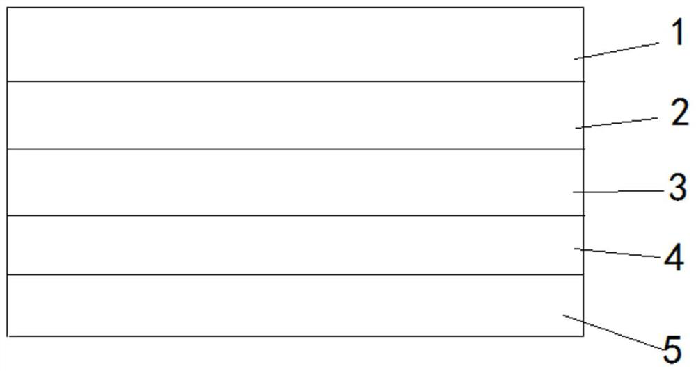
[0032] The cover provided in this embodiment, such as figure 1 As shown, including the transparent substrate 4 and the non-conductive vacuum film 3; the transparent substrate 4 includes a relatively disposed outer surface and an inner surface; the non-conductive vacuum film 3 is disposed on the outer surface, and the bottom layer of the non-conductive vacuum film 3 is single crystal. Silicon layer.
[0033] Among them, the transparent substrate 4 can be any suitable form such as glass, gem or ceramics.
[0034] The cover is used to be disposed on the mounting base, where the inner surface of the cover is used to dispose toward the mounting base, and the outer surface of the cover is used to deviate from the mounting base setting.
[0035] The cover sheet in this embodiment can be used to be disposed on the rear cover of the mobile phone, wherein the inner surface of the cover is a concave surface, and the outer surface of the cover is a convex surface.
[0036] ...
Example Embodiment
[0060] Example 2
[0061] The cover plate coating method provided in this embodiment includes the following steps:
[0062] Non-conductive vacuum film 3 is plated to the outer surface of the transparent substrate 4, and the bottom layer of the conductive vacuum film is plated into a single crystal silicon layer.
[0063] The non-conductive vacuum membrane 3 is disposed on the outer surface of the transparent substrate 4, and the user is viewed from the outside of the cover, and the color effect of the non-conductive vacuum film 3 is directly reflected to the human eye, without the need to pass through the transparent substrate 4. It can reduce the effect of the transparent substrate 4 on the display effect of the non-conductive vacuum membrane 3, and the bottom layer of the non-conductive vacuum film 3 is a single crystal silicon layer, since the single crystal silicon layer can absorb part color light, the inner surface can be The light of the part of the transparent substrate 4 ...
PUM
| Property | Measurement | Unit |
|---|---|---|
| Thickness | aaaaa | aaaaa |
| Thickness | aaaaa | aaaaa |
| Thickness | aaaaa | aaaaa |
Abstract
Description
Claims
Application Information
 - R&D Engineer
- R&D Manager
- IP Professional
- Industry Leading Data Capabilities
- Powerful AI technology
- Patent DNA Extraction
Browse by: Latest US Patents, China's latest patents, Technical Efficacy Thesaurus, Application Domain, Technology Topic.
© 2024 PatSnap. All rights reserved.Legal|Privacy policy|Modern Slavery Act Transparency Statement|Sitemap