Eureka AIR delivers breakthrough ideas for toughest innovation challenges, trusted by R&D personnel around the world.

Method of testing three-dimensional memory cell array and memory circuit

A technology of memory cells and backup memory, applied in static memory, read-only memory, digital memory information, etc., can solve problems such as affecting the overall IC performance of the operating voltage of digital devices

Pending Publication Date: 2021-09-10
TAIWAN SEMICON MFG CO LTD
View PDF0 Cites 0 Cited by
  • Summary
  • Abstract
  • Description
  • Claims
  • Application Information

AI Technical Summary

Problems solved by technology

As ICs have become smaller and more complex, the resistance of the wires in these digital devices has also changed, affecting the operating voltage of these digital devices and overall IC performance

Method used

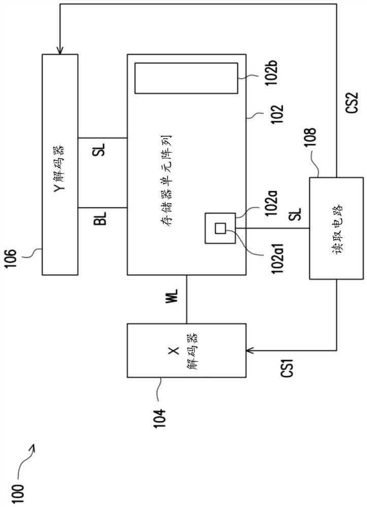
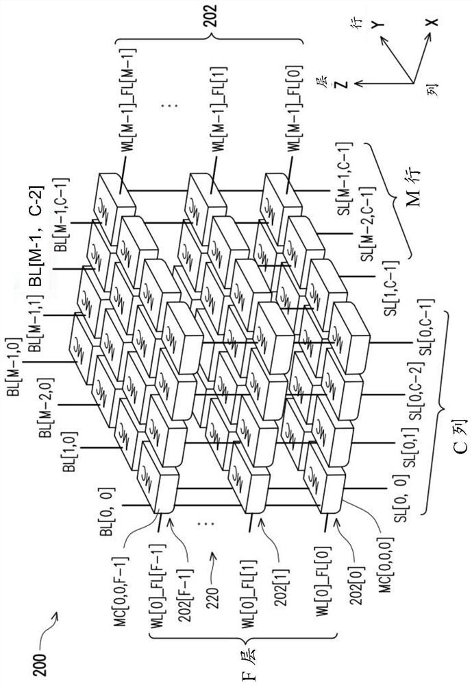
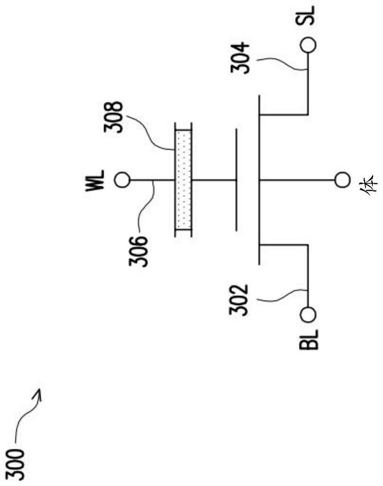

Image

  • Method of testing three-dimensional memory cell array and memory circuit
  • Method of testing three-dimensional memory cell array and memory circuit
  • Method of testing three-dimensional memory cell array and memory circuit

Examples


Embodiment Construction

[0015] The following disclosure provides many different embodiments or examples for implementing different features of the invention. Specific embodiments or examples of components and arrangements are described below to simplify the present disclosure. Of course, these are examples only and are not intended to be limiting. For example, in the following description, forming a first component over or on a second component may include an embodiment in which the first component and the second component are formed in direct contact, and may also include an embodiment in which a first component may be formed between the first component and the second component. Additional components such that the first and second components may not be in direct contact. Furthermore, the present invention may repeat reference numerals and / or letters in various examples. This repetition is for the purposes of simplicity and clarity and does not in itself indicate a relationship between the various ...


PUM


Abstract

A method of testing a three-dimensional (3D) memory cell array includes writing data to each layer of memory cells in the 3D memory cell array while performing a read operation of each memory cell in at least a first column of the 3D memory cell array, determining whether one memory cell in the 3D memory cell array malfunctions in response to the read operation, and replacing at least one malfunctioning memory cell in the 3D memory cell array with a spare memory cell in response to determining that the memory cell in the 3D memory cell array malfunctions. The first column includes memory cells on each corresponding layer of the 3D memory cell array. The embodiment of the invention also relates to a memory circuit.

Description

technical field [0001] Embodiments of the invention relate to methods and memory circuits for testing three-dimensional memory cell arrays. Background technique [0002] The semiconductor integrated circuit (IC) industry has produced a wide variety of digital devices to solve problems in many different fields. Some of these digital devices, such as memory macros, are configured for data storage. As ICs have become smaller and more complex, the resistance of the wires in these digital devices has changed, affecting the operating voltage of these digital devices and overall IC performance. Contents of the invention [0003] According to an embodiment of the present invention, there is provided a method of testing a three-dimensional (3D) memory cell array, comprising: writing data into each layer of memory cells in the 3D memory cell array; concurrently performing a read operation for each memory cell in a column, a first column comprising memory cells on each correspondin...

Claims


Application Information

Patent Timeline
IPC IPC(8): G11C29/08G11C29/50G11C11/34G11C29/12
CPCG11C29/08G11C11/34G11C29/50004G11C29/12G11C2029/5004G11C2029/5006G11C2029/1202G11C2029/1204G11C29/4401G11C29/44G11C29/04G11C29/24G11C29/50G11C29/025G11C29/56008G11C29/808G11C16/26G11C16/08G11C29/14G11C16/24G06F11/2094G11C16/10G11C29/38
Inventor 吴昭谊吕士濂杨世海
Owner TAIWAN SEMICON MFG CO LTD
Why Eureka
Eureka Blog
Learn More