
Three-dimensional chip based on system bus and three-dimensional method thereof

A system bus and three-dimensional chip technology, which is applied in the direction of electrical components, electric solid devices, circuits, etc., can solve the problem that logic chips cannot be processed in three-dimensional way

Pending Publication Date: 2021-09-28
INST OF COMPUTING TECH CHINESE ACAD OF SCI
View PDF5 Cites 0 Cited by
  • Summary
  • Abstract
  • Description
  • Claims
  • Application Information

AI Technical Summary

Problems solved by technology

Therefore, logic chips cannot be processed according to the three-dimensional thinking of memory chips

Method used


Image

  • Three-dimensional chip based on system bus and three-dimensional method thereof
  • Three-dimensional chip based on system bus and three-dimensional method thereof
  • Three-dimensional chip based on system bus and three-dimensional method thereof

Examples


Embodiment Construction

[0030] In order to make the above-mentioned features and effects of the present invention more clear and understandable, the following specific examples are given together with the accompanying drawings for detailed description as follows.

[0031] In a preferred embodiment of the present invention, a vertical stacking method of multi-layer homogeneous logic chips is proposed. These include: how to implement information communication on-chip or off-chip in the design of two or more isomorphic logic chips to complete the 3D of the chip.

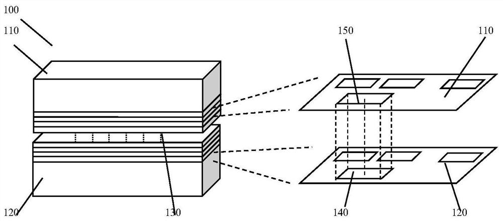
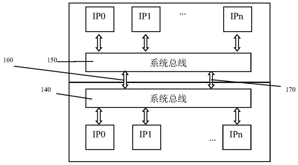
[0032] Such as Figure 1a and Figure 1b As shown, the 3D chip (100) is stacked by two isomorphic logic chips (110 and 120) in a direct bonding (130) manner (for example: DBI) through the top and top of the chip. The individual modules in the chip overlap completely. The system buses (140 and 150) in each chip are directly bonded to realize information exchange between chips, and the 3D design of the chip is completed.

[0033] Two channels...


PUM


Abstract

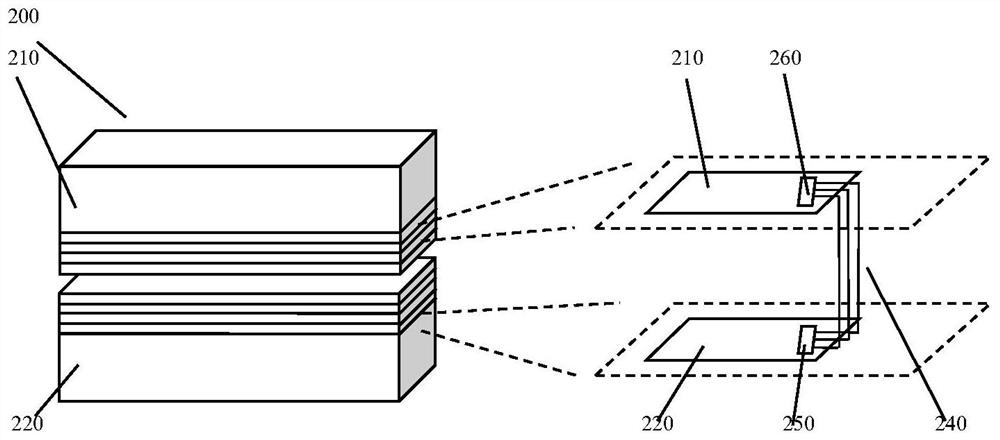
The invention provides a three-dimensional chip based on a system bus and a three-dimensional method thereof. The three-dimensional chip comprises at least two isomorphic logic chips, the isomorphic logic chips are vertically stacked with each other, and modules of the isomorphic logic chips are overlapped with each other; and the system bus in each isomorphic logic chip is connected with the system bus in the adjacent isomorphic logic chip. The communication between the isomorphic chips is realized through the structure, so that the 3D of the chips is realized.

Description

technical field [0001] The invention belongs to the field of integrated circuit chip design, and particularly relates to a three-dimensional chip based on a system bus and a three-dimensionalization method thereof. Background technique [0002] Nowadays, in the era of slowing Moore's Law, the concept of 3D chips has been proposed to increase the density of transistors. At present, many companies have realized multi-layer stacking of memory chips. How to achieve 3D for logic chips has become a topic of concern. As we all know, adopting advanced manufacturing technology means higher tape-out costs, and realizing 3D logic chips means that low-cost process technologies can be used to achieve the performance of advanced process chips. [0003] During the development of 3D chips, TSV and DBI packaging technologies have appeared one after another, which laid the foundation for the physical realization of 3D chips. Regarding how to realize 3D design of the chip, the present inven...

Claims


Application Information

Patent Timeline
IPC IPC(8): H01L23/50H01L25/065H01L21/768
CPCH01L25/0657H01L25/50H01L23/50
Inventor 王鹏超李晓霖郝沁汾叶笑春范东睿
Owner INST OF COMPUTING TECH CHINESE ACAD OF SCI
Learn More