Method for transferring a useful layer onto a support substrate
A transfer method and carrier substrate technology, applied in the field of microelectronics, can solve the problems of inhomogeneity of the useful layer 3, difficulty in eliminating inhomogeneity, etc.
- Summary
- Abstract
- Description
- Claims
- Application Information
AI Technical Summary
Problems solved by technology
Method used
Image

Examples
Embodiment Construction
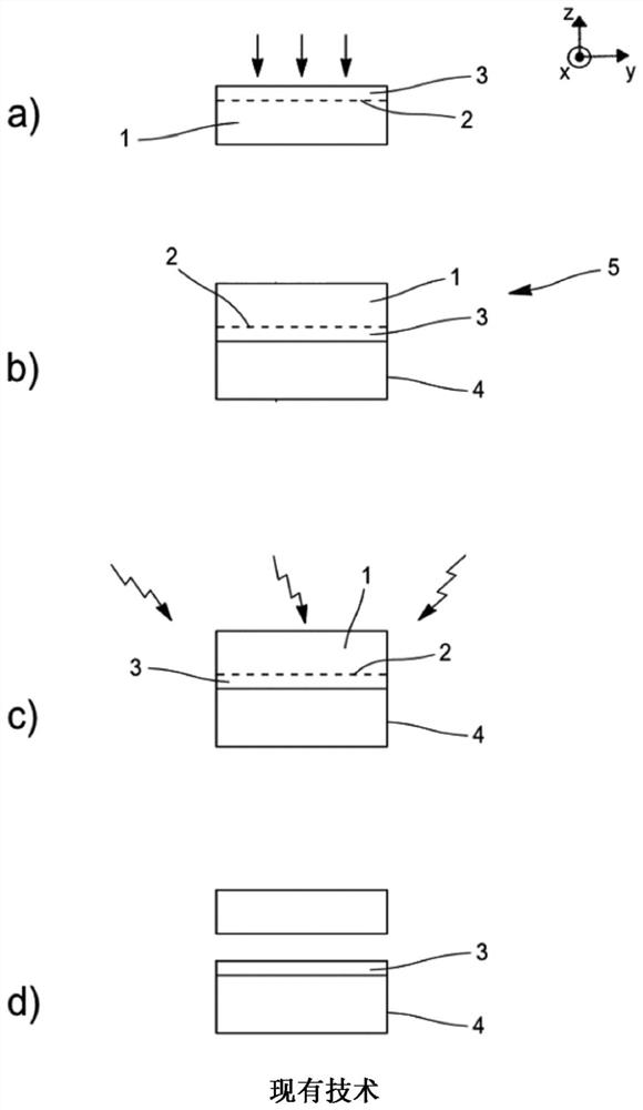
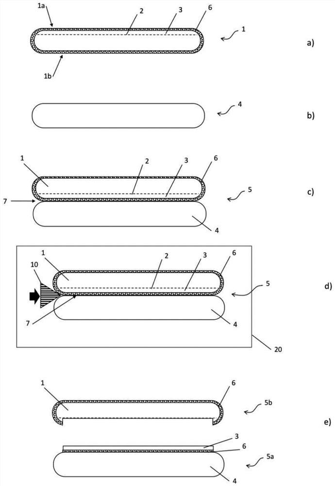
[0043] In the description, the same reference numerals may be used for the same type of elements in the drawings. The figures are schematic representations, not drawn to scale for the sake of clarity. In particular, the thicknesses of the layers along the z-axis are not proportional to the lateral dimensions along the x- and y-axes; the relative thicknesses of these layers relative to each other are not necessarily relative in the drawings. It should be noted that figure 1 The coordinate system (x,y,z) for figure 2 .
[0044] The invention relates to a method for transferring a useful layer 3 onto a carrier substrate 4 . The useful layer 3 is so named because it is intended for the production of components in the field of microelectronics or microsystems. The properties of the useful layer and the carrier substrate may vary depending on the target component type and target application. Since silicon is currently the most commonly used semiconductor material, the useful l...
PUM
 Abstract
Description
Claims
Application Information