Joining Method and Device Produced by this Method and Joining Unit

a technology of joining method and device, applied in semiconductor lasers, instruments, manufacturing tools, etc., can solve problems such as spontaneous bonding, and achieve the effects of avoiding charge-up damage, reducing bonding load, and high profile irregularity

Active Publication Date: 2008-10-09
SUGA
View PDF10 Cites 60 Cited by
  • Summary
  • Abstract
  • Description
  • Claims
  • Application Information

AI Technical Summary

Benefits of technology

[0113]In a bonding method of bonding a plurality of objects to be bonded having a metal bonding surface at low temperature, room-temperature bonding can be performed in the atmospheric air. Direct bonding can be obtained without a high profile irregularity which is required by conventional room-temperature bonding.
[0114]At least one of the objects to be bonded may be a semiconductor, and the bonding surface of each of the objects to be bonded may be subjected to plasma cleaning using the low-pressure plasma which is generated with electric field having alternating + and − directions generated by an alternating power supply before the cleaned bonding surfaces are bonded together in a solid phase at room temperature. Thereby, the + ion and the − electron can be caused to alternately strike the object to be bonded so as to neutralize before accumulating charge. Thereby, it is possible to avoid charge-up damage. By adjusting the times of the + region and the − region using a bias voltage Vdc or the pulse width of pulsed waves, an optimum region for neutralization can be created.
[0115]In the bonding method of bonding a plurality of objects to be bonded having a metal bonding surface formed of gold or copper at low temperature, room-temperature bonding can be performed in the atmospheric air. Also, a bonding load can be reduced.
[0116]In a chamber having a reduced pressure, both objects to be bonded are shifted to side positions so that the bonding surfaces do not overlap each other, and after both the bonding surfaces are subjected to plasma cleaning, the objects to be bonded are shifted to positions which allow both the bonding surfaces to face each other, and at least one of the objects to be bonded is shifted in a direction substantially perpendicular to the bonding surface of

Problems solved by technology

This is because the profile irregularity of the order of several nanometer

Method used


Image

  • Joining Method and Device Produced by this Method and Joining Unit
  • Joining Method and Device Produced by this Method and Joining Unit
  • Joining Method and Device Produced by this Method and Joining Unit

Examples


first embodiment

[0164]Hereinafter, a first embodiment of the present invention will be described with reference to the drawings. FIG. 15 illustrates the first embodiment of a bonding apparatus according to the present invention. In this embodiment, an apparatus for bonding a chip 20 formed of a semiconductor (first object to be bonded) and a substrate 22 (second object to be bonded) will be described as an example. A bonding surface of the chip 20 has a metal electrode 20a which is an electrode and is formed of gold, and a bonding surface of the substrate 22 has a metal electrode 22a which is an electrode and is provided at a position which allows to face the metal electrode 20a of the chip. The metal electrode 20a of the chip and the metal electrode 22a of the substrate are bonded together by pressing.

[0165]The bonding apparatus roughly includes a bonding mechanism 27 including a vertical drive mechanism 25 and a head section 26, a mounting mechanism 28 including a stage 10 and a stage table 12, a...

second embodiment

[0171]Next, a second embodiment of the bonding apparatus of the present invention will be described in detail with reference to FIGS. 16A and 16B. This embodiment is significantly different from the above-described first embodiment in that a bonding portion of an object to be bonded is constructed by forming a gold film on a surface of a base material formed of a metal, and other parts of this embodiment are similar to those of the first embodiment. Hereinafter, the second embodiment will be described in detail, mainly in terms of the difference from the first embodiment. Note that the same configuration and operation as those of the first embodiment will not be described.

[0172]In the second embodiment, bonding portions of the chip 20 and the substrate 22 are formed as metal bumps as follows. Specifically, a plurality of coppers are used as base materials 20b and 22b, and gold films 20c and 22c are formed on surfaces of the base materials 20b and 22b. The metal bumps are subjected t...

third embodiment

[0174]Next, a third embodiment of the bonding apparatus of the present invention will be described in detail. This embodiment is significantly different from the above-described first and second embodiments in that minute irregularities are formed on a surface of a bonding portion, and other parts and operations of this embodiment are similar to those of the first and second embodiments, and will not be described. Hereinafter, specific features of this embodiment will be described in detail.

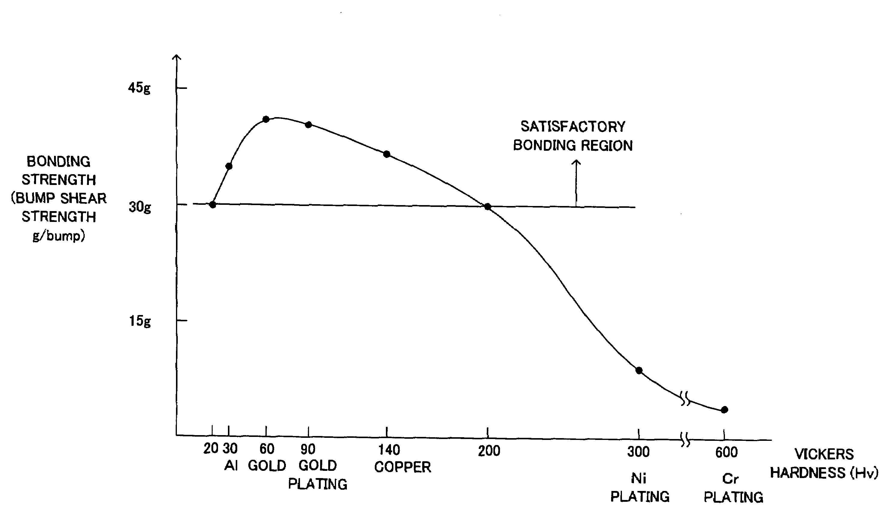
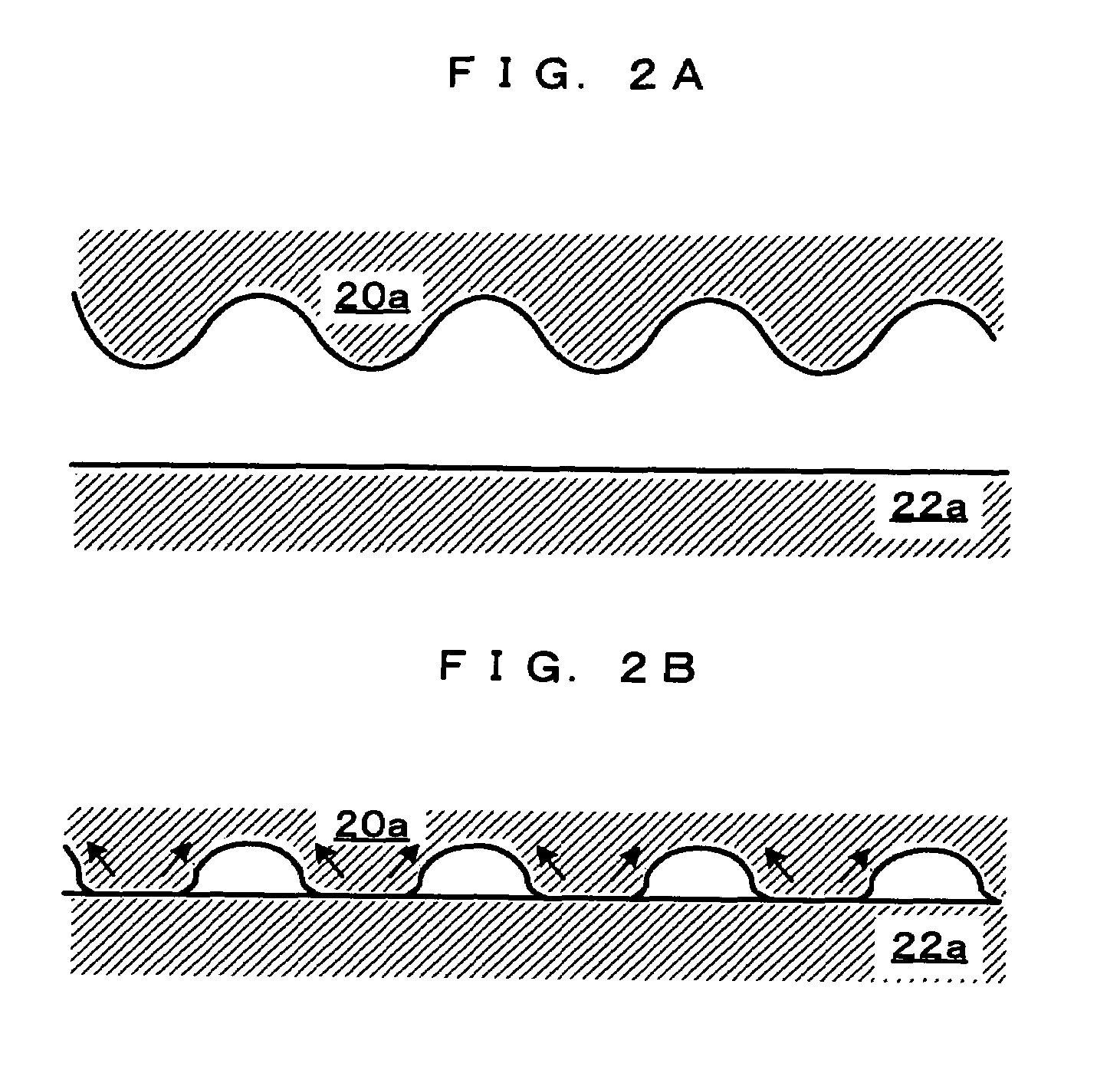
[0175]According to this embodiment, the convex portions are crushed by pressing when objects to be bonded are bonded as illustrated in FIGS. 2A and 2B and are then caused to be spread, so that a new surface appears and bonding is achieved. When viewed microscopically, crystal orientations arranged as illustrated in FIGS. 3A and 3B are rotated by the convex portion being crushed, so that the new surface appears. As can be seen from FIG. 4, when the surface roughness (minute irregularities) is 120 ...


PUM

PropertyMeasurementUnit
Lengthaaaaaaaaaa
Surface roughnessaaaaaaaaaa
Temperatureaaaaaaaaaa

Abstract

A practical bonding technique is provided for solid-phase room-temperature bonding which does not require a profile irregularity of the order of several nanometers, in which a high-vacuum energy wave treatment and continuous high-vacuum bonding are not required.
Since an adhering substance layer is thin immediately after a surface activating treatment using an energy wave, a bonding interface is spread by crushing the adhering substance layer to perform bonding, so that a new surface appears on a bonding surface, and objects to be bonded are bonded together. In order to crush the adhering substance layer more easily, a bonding metal of a bonding portion of the object to be bonded needs to have a low hardness. According to the results of various experiments conducted by the present inventors, it was found that the hardness of the bonding portion which is a Vickers hardness of 200 Hv or less is particularly effective for room-temperature bonding.

Description

TECHNICAL FIELD[0001]The present invention relates to a bonding technique for bonding a plurality of objects to be bonded having a metal bonding portion at room temperature.BACKGROUND ART[0002]Conventionally, room-temperature bonding methods are performed in a vacuum as described in Patent Document 1 or in inert gas as described in Patent Document 2 after a bonding surface is cleaned using an energy wave. This is because, if the bonding surface is exposed to the atmospheric air, oxidation or readhesion of organic substances or the like prevents metal atoms from being attracted by each other.[0003]In the case of Patent Document 2, if gold is used, which does not react, oxidation is prevented, but adhesion of organic substances remains. Therefore, bonding is performed in inert gas.[0004]The bonding surface is polished to a profile irregularity of the order of several nanometers before being subjected to bonding under a low load. This is because the profile irregularity of the order of...

Claims


Application Information

Patent Timeline
IPC IPC(8): B23K20/00B23K31/02H05K7/00H01L21/60H01L21/603H01S5/0238
CPCB23K20/023B23K20/16B23K20/22B23K20/233B23K2201/42B23K2203/12G02B6/4214G02B6/4232H01L21/67092H01L21/67144H01L24/75H01L24/81H01L24/97H01L25/0657H01L25/50H01L2224/13144H01L2224/13147H01L2224/16H01L2224/48463H01L2224/75H01L2224/75252H01L2224/75822H01L2224/7592H01L2224/81009H01L2224/81054H01L2224/81121H01L2224/81205H01L2224/81208H01L2224/81224H01L2224/81801H01L2224/81894H01L2224/97H01L2225/06513H01L2924/01002H01L2924/01004H01L2924/01013H01L2924/01015H01L2924/01018H01L2924/01029H01L2924/01058H01L2924/01074H01L2924/01075H01L2924/01077H01L2924/01078H01L2924/01079H01L2924/01082H01L2924/19041H01S5/02252H01S5/02268H01S5/02272H01S5/02284H01S5/02292H01L2224/0558H01L2224/05644H01L2924/01005H01L2924/01006H01L2924/01019H01L2924/01023H01L2924/01024H01L2924/01033H01L2924/0105H01L2924/01068H01L2924/014H01L2924/12041H01L2224/81013H01L2224/8183H01L2224/0401H01L2924/1461H01L2924/00014H01L2224/81H01L2924/00B23K2101/42B23K2103/12H01S5/02375H01S5/02326H01S5/0237H01S5/02255H01S5/02251H01S5/0238
Inventor SUGAOKADA, MASUAKI
Owner SUGA
Why Eureka
Try Eureka