Apparatus and method for plasma processing

a plasma processing and apparatus technology, applied in the direction of electrical apparatus, electrical discharge tubes, decorative arts, etc., can solve the problem of limit to the prevention of charging damage, achieve low damage to the processed body, reduce the distance between the voltage application electrode and the ground electrode, and achieve high etching capability

Inactive Publication Date: 2009-11-26
TOKYO ELECTRON LTD
View PDF3 Cites 0 Cited by
  • Summary
  • Abstract
  • Description
  • Claims
  • Application Information

AI Technical Summary

Benefits of technology

[0004]For example, conventionally known techniques of this type are disclosed in Japanese Patent Laid-Open Publication No. Hei 7-201496 (claims 3 and 9, and Paragraphs [0010], [0031], and [0037]), Japanese Patent Laid-Open Publication No. Sho 61-265820 (claim 1, Lines 6 to 13 on the top right column on page 2, Line 5 on the top left column on page 3 to line 2 on the bottom left column on the same page, and the column stating the Effects of the Invention), and Japanese Patent No. 3113786 (claims 1 and 2, and Paragraphs [0029] and [0030]) (hereinafter, referred to as references 1 to 3, respectively).
[0005]The reference 1 suggests an apparatus and a method for generating plasma. This apparatus includes a voltage application electrode for being applied high-frequency power, a ground electrode, and a distance adjusting mechanism for variably adjusting the distance between these electrodes. When a voltage is applied to the voltage application electrode, the distance between the voltage application electrode and the ground electrode is reduced to such an extent as to readily provide an igniting in accordance with the Paschen's law. After plasma has been produced, the distance between these electrodes is then increased, thereby ensuring a high etching capability and low damage to the processed body at the same time.
[0006]On the other hand, since the distance control mechanism for adjusting the distance between the upper and lower electrodes makes the apparatus complicated, the reference 2 suggests a plasma processing apparatus that requires no distance control mechanism. This plasma processing apparatus has two electrodes, which are isolated from each other and each connected with an individual high-frequency power supply, and the distances between these electrodes and a ground electrode disposed to face these electrodes are different. With this apparatus, the high-frequency power applied to an electrode spaced apart farther from the ground electrode is stopped immediately after a discharge is initiated, thereby allowing for readily initiating a discharge at a low voltage even for high-rate etching. In other words, different electrodes are used for plasma igniting and plasma processing.
[0007]On the other hand, the reference 3 suggests a plasma processing apparatus with a two-frequency application scheme to apply respective high-frequency powers to the upper and lower electrodes. With this apparatus, the ON or OFF timing of the high-frequency powers applied to both the upper and lower electrodes is controlled to alleviate charging damage.
[0008]However, in the conventional plasma processing methods as suggested in the references 1 and 2, the distance between the upper and lower electrodes was optimized each at the time of plasma igniting and during plasma processing to alleviate charging damage and optimize the plasma processing at the same time. However, significant progress was made since then toward finer-line and thinner-film processes for semiconductor devices followed by significant improvements in plasma processing apparatuses. This resulted in only the distance between the electrodes being optimized each at the time of plasma igniting and during plasma processing, yet causing a limitation to the prevention of charging damage.
[0009]The present invention was developed to solve the aforementioned problem. It is therefore an object of the invention to provide an apparatus and a method for plasma processing which can prevent charging damage to objects to be processed even when progress will be made toward finer-line and thinner-film processes for semiconductor devices.SUMMARY OF THE INVENTION

Problems solved by technology

This resulted in only the distance between the electrodes being optimized each at the time of plasma igniting and during plasma processing, yet causing a limitation to the prevention of charging damage.

Method used


Image

  • Apparatus and method for plasma processing
  • Apparatus and method for plasma processing
  • Apparatus and method for plasma processing

Examples


Embodiment Construction

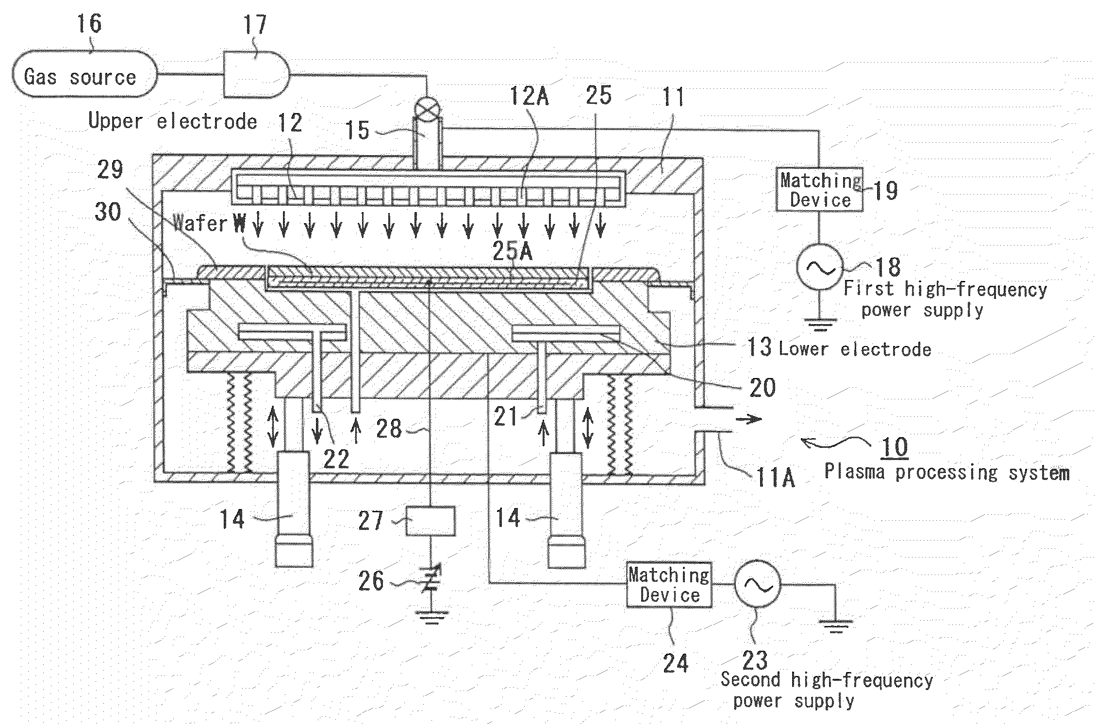
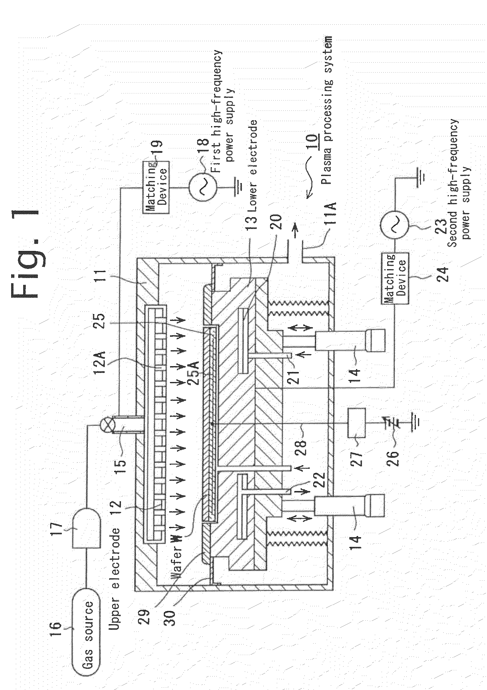
[0028]The inventors decided to thoroughly address the present charging damage. To this end, for example, a parallel plate plasma processing apparatus with the two-frequency application scheme was used for applying high-frequency powers to the upper and lower electrodes at different frequencies, respectively. With this apparatus, the distance between the upper and lower electrodes was optimized. Under this condition, plasma igniting, plasma processing (etching), and plasma extinction are performed on a wafer to determine the distribution of breakdown voltages of an antenna MOS (with an antenna ratio of one million). Consequently, as shown by the shaded lines illustrated in FIG. 5, defective devices due to a breakdown in the gate insulating film were found at the central portion and periphery of the wafer, resulting in up to a yield of 45%.

[0029]In this regard, the inventors employed CHARM®-2 wafer (Wafer Charging Monitors, Inc.) for monitoring charging of wafer to determine the perce...


PUM

PropertyMeasurementUnit
frequencyaaaaaaaaaa
frequencyaaaaaaaaaa
temperaturesaaaaaaaaaa

Abstract

At the time of plasma igniting or during plasma processing, only optimizing the distance between electrodes in each case caused a limitation to the prevention of charging damage. To resolve this, a novel plasma processing method employs a plasma processing apparatus which includes an upper electrode to which first high-frequency power is applied, a lower electrode to which second high-frequency power is applied, and a lift mechanism for controlling the spacing between the upper and lower electrodes. The first high-frequency power is applied to the upper electrode to cause plasma igniting. The method is adapted to make the spacing between the upper and lower electrodes larger at least at the time of plasma extinction than during plasma processing of a wafer on the lower electrode.

Description

BACKGROUND OF THE INVENTION[0001]1. Field of the Invention[0002]The present invention relates to an apparatus and a method for plasma processing and more particularly to an apparatus and a method for plasma processing which can reduce charging damage to objects to be processed being plasma processed using the plasma processing apparatus such as a parallel plate plasma processing apparatus.[0003]2. Description of the Related Art[0004]For example, conventionally known techniques of this type are disclosed in Japanese Patent Laid-Open Publication No. Hei 7-201496 (claims 3 and 9, and Paragraphs [0010], [0031], and [0037]), Japanese Patent Laid-Open Publication No. Sho 61-265820 (claim 1, Lines 6 to 13 on the top right column on page 2, Line 5 on the top left column on page 3 to line 2 on the bottom left column on the same page, and the column stating the Effects of the Invention), and Japanese Patent No. 3113786 (claims 1 and 2, and Paragraphs [0029] and [0030]) (hereinafter, referred ...

Claims


Application Information

Patent Timeline
Patent Type & Authority Applications(United States)
IPC IPC(8): H01L21/3065H01J37/32
CPCH01J37/32568H01J37/32082
Inventor MORIMOTO, TAMOTSUMURAKAMI, TAKAHIRO
Owner TOKYO ELECTRON LTD
Why Eureka
Try Eureka