Semiconductor device and method for manufacturing the same

a semiconductor and device technology, applied in semiconductor devices, semiconductor/solid-state device details, electrical equipment, etc., can solve the problems of difficult removal of charges injected as a result of a charge-up phenomenon during a diffusion process, memory element cannot be protected from a charge-up, and the protection effect is not achieved

Active Publication Date: 2009-03-26
PANNOVA SEMIC
View PDF24 Cites 1 Cited by
  • Summary
  • Abstract
  • Description
  • Claims
  • Application Information

AI Technical Summary

Benefits of technology

[0013]The semiconductor device of the present invention makes it possible to avoid the occurrence of charge-up damage to the protection target element from a point of time when the conductive film serving as the protection target element electrode is formed. The fuse film is configured to be torn by applying a predetermined current thereto. The tearing of the fuse film after the diffusion process makes it possible to apply high positive and negative voltages required for driving the protection target element.
[0015]According to the method for manufacturing the semiconductor device of the present invention, the protection target element is protected from charge-up damage from a point of time when the electrode of the protection target element is formed. After the completion of the diffusion process, high positive and negative voltages required for driving the protection target element can be applied.

Problems solved by technology

In nonvolatile memories involving local charge accumulation, charges injected as a result of a charge-up phenomenon during a diffusion process are often difficult to remove after the completion of the diffusion process.
According to the aforementioned conventional technique, however, the protection effect is achieved only after the wiring process.
Therefore, the memory element cannot be protected from a charge-up phenomenon caused during a diffusion process on a Front End of Line (FEOL) level.
Further, a negative bias cannot be applied to the protection target element after the diffusion process.
Specifically, since low-temperature processes are required under the fine design rules, a heating process for withdrawing charges stored on the FEOL level cannot be performed.
As a result, the charge-up damage is not suppressed to a sufficient degree by measures taken to protect the memory element in the processes after the wiring process.

Method used


Image

  • Semiconductor device and method for manufacturing the same
  • Semiconductor device and method for manufacturing the same
  • Semiconductor device and method for manufacturing the same

Examples


embodiment 1

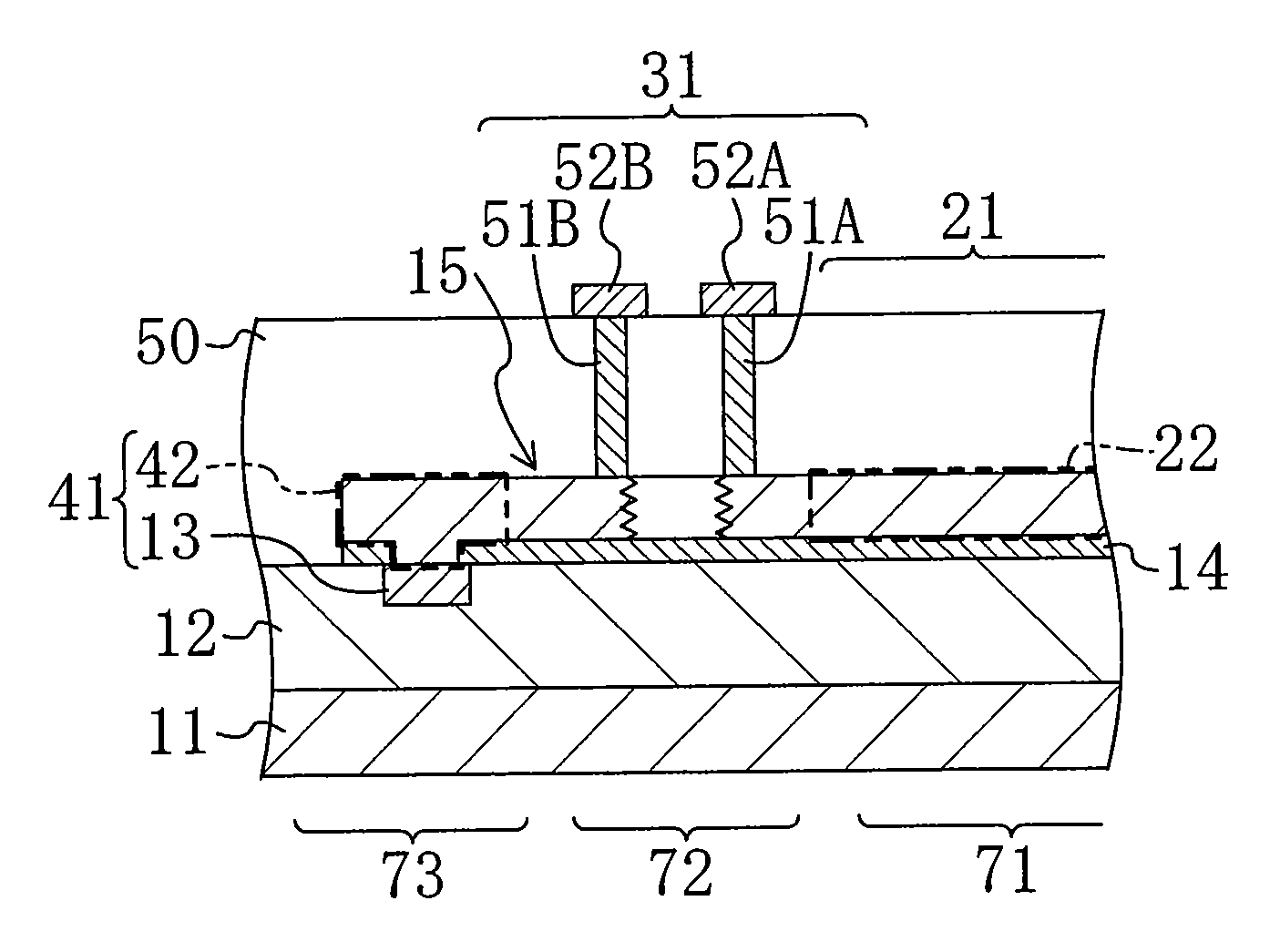
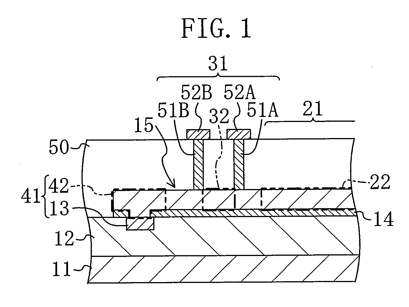
[0030]Embodiment 1 of the present invention is described below with reference to the drawings. FIG. 1 shows a sectional structure of a semiconductor device of Embodiment 1. As shown in FIG. 1, the semiconductor device of the present embodiment includes a protection target element 21, a fuse structure 31 and a substrate connecting part 41.

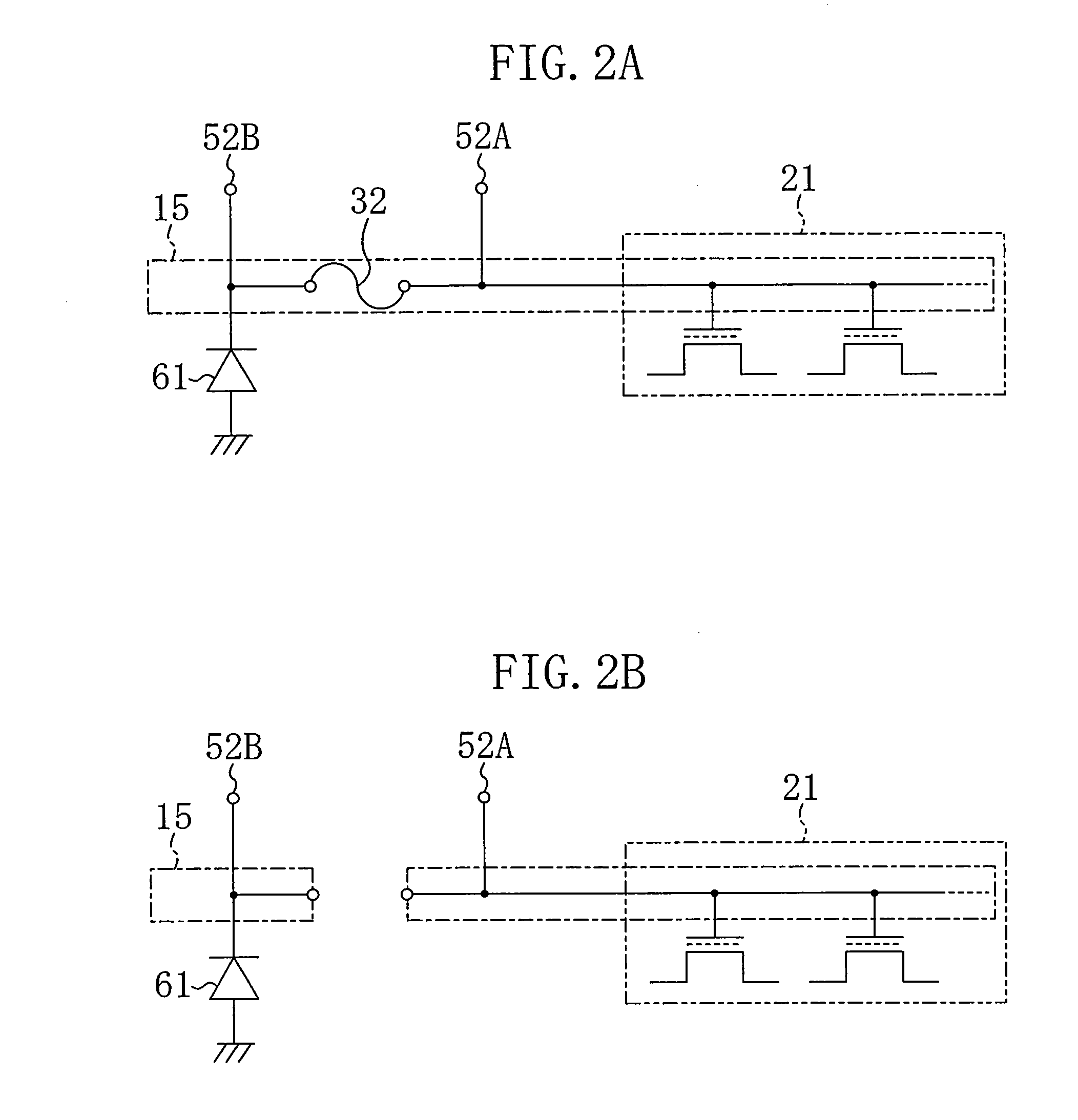
[0031]The protection target element 21 is, for example, a nonvolatile memory formed on a first conductivity type semiconductor substrate 11 made of silicon (Si). In FIG. 1, only part of the protection target element 21 is shown, i.e., a protection target element electrode 22. The protection target element electrode 22 may be, for example, a gate electrode of a memory element. The fuse structure 31 has a fuse film 32 which is configured to be torn by applying a current thereto. The substrate connecting part 41 includes a substrate connecting electrode 42 connected to the semiconductor substrate 11.

[0032]The protection target element electrode 22, the...

embodiment 2

[0051]Embodiment 2 of the present invention is described with reference to the drawings.

[0052]FIG. 8 shows a sectional structure of a semiconductor device of Embodiment 2. In FIG. 8, like reference numerals are used to refer to like elements shown in FIG. 1 so as to avoid repetition of the description.

[0053]In the semiconductor device of Embodiment 2, a conductive film 15 includes a lower conductive film 15A and an upper conductive film 15B. A fuse film 32 does not include the lower conductive film 15A but is made of only the upper conductive film 15B formed on a fuse insulating film 33.

[0054]According to the semiconductor device of Embodiment 2, part of the conductive film corresponding to the fuse film 32 is reduced in thickness to increase the resistance.

[0055]Therefore, as compared with the semiconductor device of Embodiment 1, the fuse film 32 is torn more easily.

[0056]Hereinafter, a method for manufacturing the semiconductor device of Embodiment 2 is described with reference t...


PUM


Abstract

A semiconductor device includes a protection target element formed on a semiconductor substrate and includes a protection target element electrode, a substrate connecting part including a substrate connecting electrode electrically connected to the semiconductor substrate and a fuse structure provided between the protection target element electrode and the substrate connecting electrode and includes a fuse film configured to be torn by applying a predetermined current thereto. The protection target element electrode, the substrate connecting electrode and the fuse film are formed of an integral conductive film as long as the fuse film is not torn.

Description

CROSS-REFERENCE TO RELATED APPLICATION[0001]This non-provisional application claims priority under 35 U.S.C. §119(a) of Japanese Patent Application No. 2007-245928 filed in Japan on Sep. 21, 2007, the entire contents of which are hereby incorporated by reference.BACKGROUND OF THE INVENTION[0002]1. Field of the Invention[0003]The present invention relates to a semiconductor device and a method for manufacturing the same. In particular, it relates to a semiconductor device, such as a memory device which is disadvantageously affected by a charge-up phenomenon during a diffusion process, and a method for manufacturing the same.[0004]2. Description of Related Art[0005]In nonvolatile memories involving local charge accumulation, charges injected as a result of a charge-up phenomenon during a diffusion process are often difficult to remove after the completion of the diffusion process. For this reason, greater importance has been placed on a technology for suppressing charge-up damage to a...

Claims


Application Information

Patent Timeline
Patent Type & Authority Applications(United States)
IPC IPC(8): H01L27/115H01L21/8247
CPCH01L23/5256H01L27/0251H01L27/11517H01L27/11568H01L2924/0002H01L27/1052H01L2924/00H10B99/00H10B41/00H10B43/30
Inventor HIGUCHI, YUICHIROTAKAHASHI, KEITA
Owner PANNOVA SEMIC
Why Eureka
Try Eureka