Capacitive coupling plasma processing apparatus

a plasma processing and coupling technology, applied in the direction of electric discharge tubes, chemical vapor deposition coatings, coatings, etc., can solve the problems of poor planar uniformity, charge-up damage, and difficulty in controlling plasma uniformity, so as to prevent charge-up damage and high planar uniformity of plasma processing

Active Publication Date: 2010-08-03
KIOXIA CORP +1
View PDF8 Cites 5 Cited by
  • Summary
  • Abstract
  • Description
  • Claims
  • Application Information

AI Technical Summary

Benefits of technology

[0013]An object of the present invention to provide a plasma processing apparatus of the capacitive coupling type, which brings about a high planar uniformity of plasma processing, and prevents charge-up damage.
[0022]In the apparatus according to the first aspect, when plasma is generated in the chamber, an electric current flows from the plasma to the functional surface disposed around the target substrate. In this case, the plasma is expanded outward and thereby results in a uniform electron density distribution. Consequently, it is possible to improve the planar uniformity of the plasma process, and reduce the charge-up damage.

Problems solved by technology

However, where a lower pressure and lower ion energy are used, as described above, it becomes difficult to control the plasma uniformity because of increase in plasma resistivity.
As a result, the uniformity of the plasma density is further deteriorated, which brings about a poor planar uniformity and charge-up damage in plasma processing, such as etching
However, the high resistivity member employed for the main surface central portion of an RF application electrode may consume too much RF power as Joule heat (energy loss), resulting in a low efficiency.

Method used


Image

  • Capacitive coupling plasma processing apparatus
  • Capacitive coupling plasma processing apparatus
  • Capacitive coupling plasma processing apparatus

Examples


first embodiment

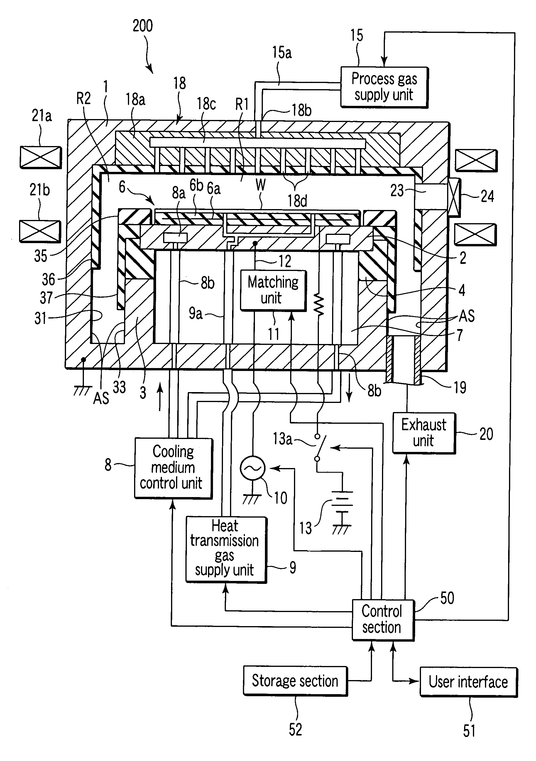
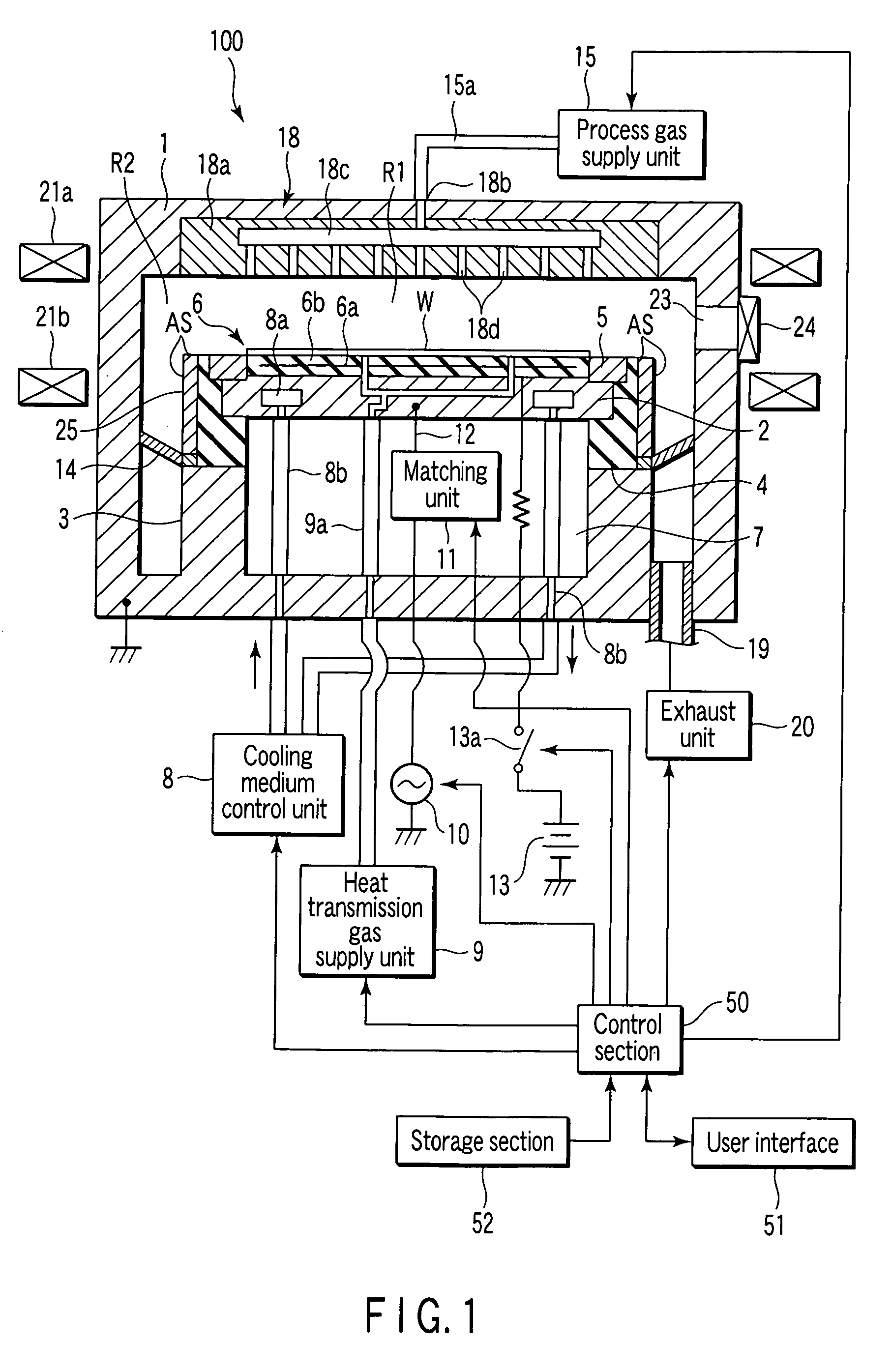
[0044]FIG. 1 is a sectional view showing a plasma etching apparatus as a plasma processing apparatus according to a first embodiment of the present invention. This apparatus is arranged to etch an oxide film (SiO2 film) disposed on a semiconductor wafer.

[0045]This plasma etching apparatus 100 includes an airtight process chamber 1 having an essentially cylindrical shape. For example, the chamber 1 has a main body made of a metal, such as aluminum, with an inner surface covered with an insulating film formed thereon, such as an oxidization processed film, or insulative ceramic film of, e.g. Y2O3 (for example, a thermal spraying film). The chamber 1 is grounded.

[0046]A support table 2 is disposed in the chamber 1 and configured to horizontally support a target substrate or wafer W and to also serve as a lower electrode. For example, the support table 2 is made of aluminum with an oxidization processed surface. A support portion 3 having a ring shape extends upward from the bottom of t...

experiment 1

[0081]At first, using an apparatus of the same basic structure as that shown in FIG. 1, a plasma process was performed with the shield member 25 at different heights, and the self-bias voltage Vdc of plasma was measured to check the planar fluctuation thereof. The shield member 25 was made of aluminum covered with an anodized film formed on the surface. Three present examples A, B, and C according to the first embodiment were prepared to set the upper end of the shield member at different heights, and examined. In the present example A, the height of the upper end of the shield member was set to be the same as that of the upper end of the support table (Z=0). In the present example B, the height of the upper end of the shield member was set to be 4.5 mm above the support table, i.e. almost the same as the height of the wafer surface (Z=+4.5). In the present example C, the height of the upper end of the shield member was set to be 9.5 mm above the support table (Z=+9.5). Further, for...

experiment 2

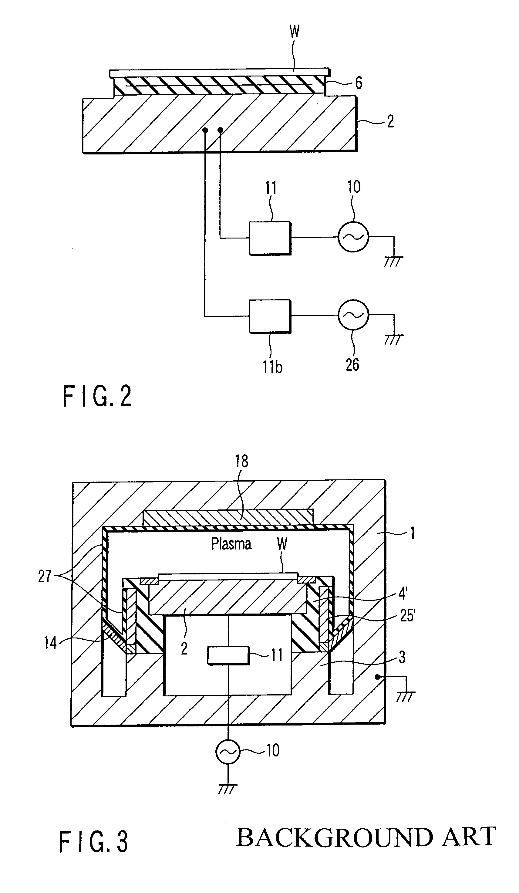
[0085]Next, the effect of the exhaust ring was examined, while the shield member was set at a height of Z=0. Two present examples E and F according to the first embodiment were prepared with different structures of the exhaust ring. In the present example E (which was the same as the present example A), a conical exhaust ring was used, as shown in FIG. 1 (having a height of −30 to −110 mm and covered with an insulating film). In the present example F, an exhaust ring was disposed near the bottom of the chamber as shown in FIG. 7 (having a height of −170 mm), while the exhaust ring was prepared to provide a functional surface to be coupled with plasma in a sense of DC. The plasma process was performed on a 300 mm wafer under the same conditions as the experiment 1. The self-bias voltage Vdc at positions directly above the wafer was measured by a Vdc monitor built in the matching unit to obtain the planar distribution of Vdc.

[0086]The results of this experiment are shown in FIGS. 10 a...


PUM

PropertyMeasurementUnit
frequencyaaaaaaaaaa
magnetic fieldaaaaaaaaaa

Abstract

A capacitive coupling plasma processing apparatus includes a process chamber configured to have a vacuum atmosphere, and a process gas supply section configured to supply a process gas into the chamber. In the chamber, a first electrode and a second electrode are disposed opposite each other. An RF power supply is disposed to supply an RF power to the first or second electrode to form an RF electric field within a plasma generation region between the first and second electrodes, so as to turn the process gas into plasma. The target substrate is supported by a support member between the first and second electrodes such that a process target surface thereof faces the second electrode. A conductive functional surface is disposed in a surrounding region around the plasma generation region and grounded to be coupled with the plasma in a sense of DC to expand the plasma.

Description

CROSS-REFERENCE TO RELATED APPLICATIONS[0001]This application claims the benefit of U.S. Provisional Application No. 60 / 658,155, filed Mar. 4, 2005.[0002]This application is based upon and claims the benefit of priority from prior Japanese Patent Applications No. 2004-350998, filed Dec. 3, 2004; and No. 2005-330251, filed Nov. 15, 2005, the entire contents of both of which are incorporated herein by reference.BACKGROUND OF THE INVENTION[0003]1. Field of the Invention[0004]The present invention relates to a plasma processing apparatus of the capacitive coupling type, used for performing a plasma process on a target substrate in, e.g. a semiconductor processing system. The term “semiconductor process” used herein includes various kinds of processes which are performed to manufacture a semiconductor device or a structure having wiring layers, electrodes, and the like to be connected to a semiconductor device, on a target substrate, such as a semiconductor wafer or a glass substrate use...

Claims


Application Information

Patent Timeline
Patent Type & Authority Patents(United States)
IPC IPC(8): C23F1/00H01L21/306C23C16/00
CPCH01J37/32082H01J37/32697
Inventor HIMORI, SHINJIIMAI, NORIAKIHORIGUCHI, KATSUMINEZU, TAKAAKIMATSUYAMA, SHOICHIROMATSUMARU, HIROKIHAYAMI, TOSHIHIRONAGASEKI, KAZUYASAKAI, ITSUKOOHIWA, TOKUHISASUGIYASU, YOSHIKAZU
Owner KIOXIA CORP
Why Eureka
Try Eureka