Capacitive coupling plasma processing apparatus

a plasma processing and coupling technology, applied in the direction of vacuum evaporation coating, chemical vapor deposition coating, coating, etc., can solve the problems of complex apparatus structure, less uniform processing, charge-up damage, etc., and achieve the effect of preventing charge-up damage and high planar uniformity of plasma processing

Active Publication Date: 2011-12-06
TOKYO ELECTRON LTD
View PDF15 Cites 11 Cited by
  • Summary
  • Abstract
  • Description
  • Claims
  • Application Information

AI Technical Summary

Benefits of technology

[0015]An object of the present invention to provide a plasma processing apparatus of the capacitive coupling type, which brings about a high planar uniformity of plasma processing, and prevents charge-up damage.
[0031]In the apparatus according to the first and second aspects, the spatial electric potential distribution is uniformized, so that the substrate receives ion energy incident thereon with a uniform distribution. Further, the uniform ion energy brings about uniform electron energy in plasma generation, thereby resulting in a uniform electron density distribution. Consequently, it is possible to improve the planar uniformity of the etching process, and to reduce the charge-up damage, such as dielectric breakdown of gate oxide films.

Problems solved by technology

Specifically, in conventional apparatuses using high ion energy, poor planar uniformity of plasma potential does not cause a serious problem.
However, as the pressure and ion energy are set to be lower, poor planar uniformity of plasma potential can easily make the process less uniform and easily cause charge-up damage.
However, the technique of Patent Document 1 requires the current path reform means or impedance adjusting means and thus makes the apparatus structure complicated.
Further, this technique is not necessarily sufficient in the planar uniformity of plasma processing.

Method used


Image

  • Capacitive coupling plasma processing apparatus
  • Capacitive coupling plasma processing apparatus
  • Capacitive coupling plasma processing apparatus

Examples


Embodiment Construction

[0055]Embodiments of the present invention will now be described with reference to the accompanying drawings. In the following description, the constituent elements having substantially the same function and arrangement are denoted by the same reference numerals, and a repetitive description will be made only when necessary.

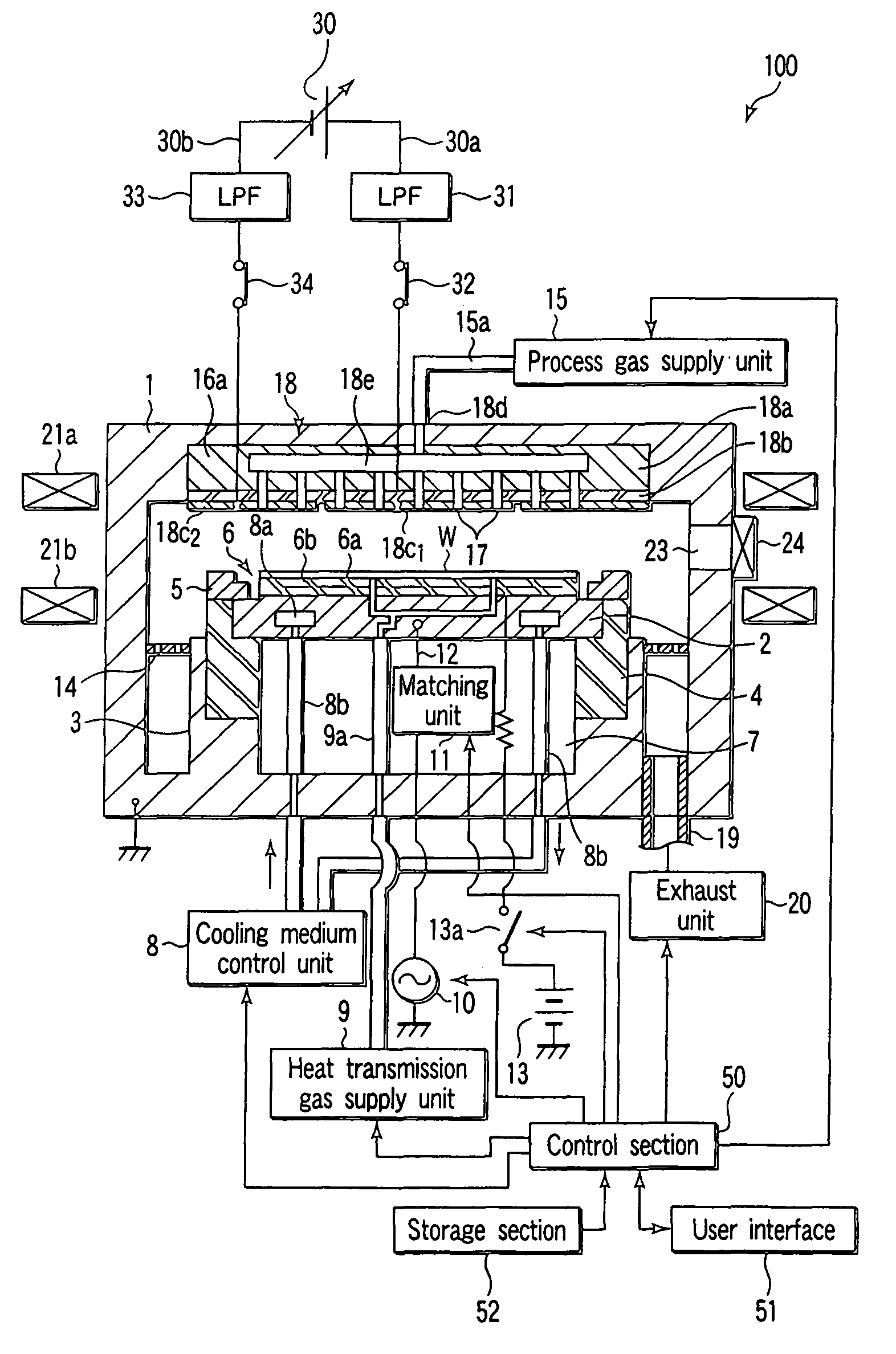
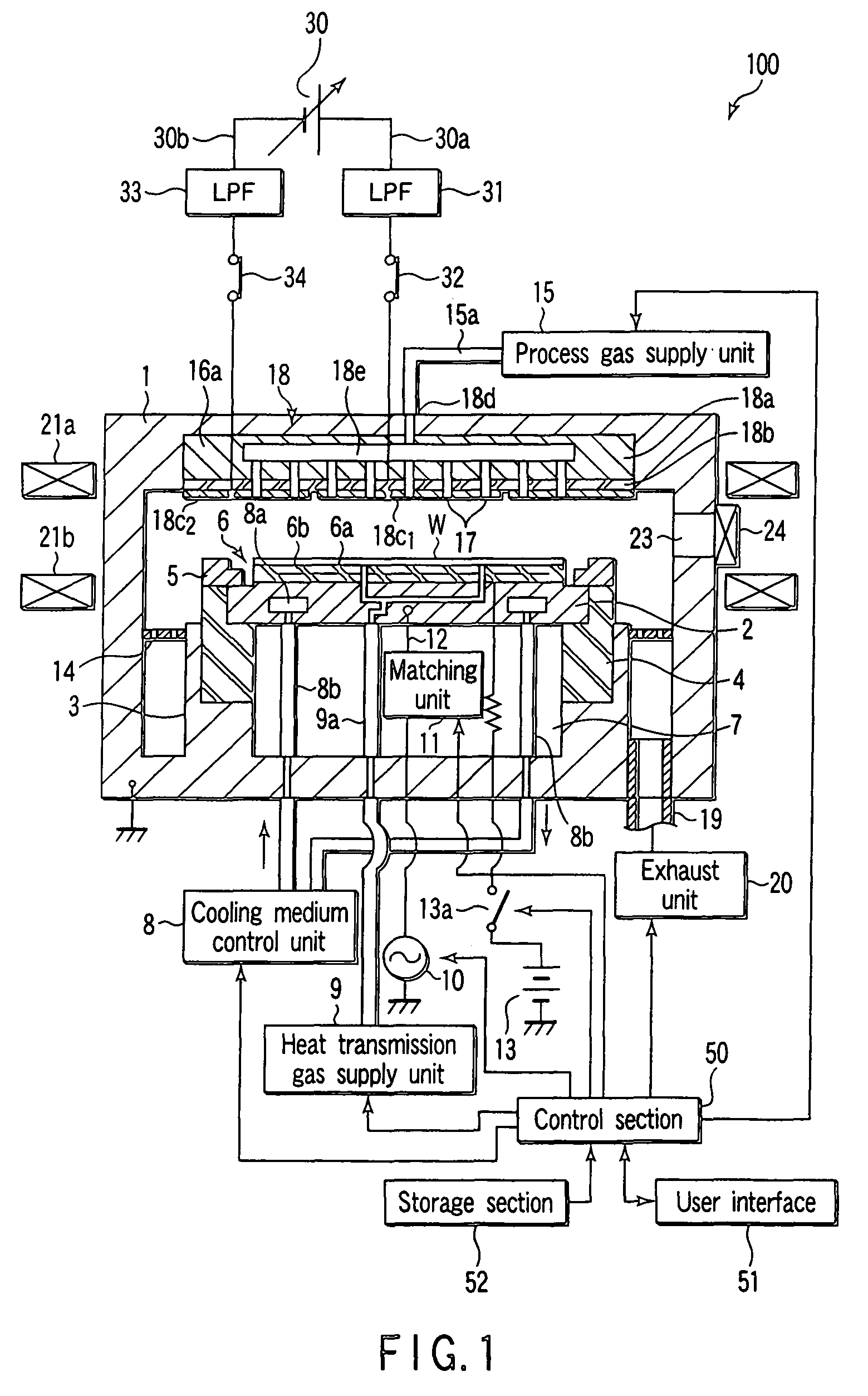
[0056]FIG. 1 is a sectional view showing a plasma etching apparatus as a plasma processing apparatus according to an embodiment of the present invention.

[0057]This plasma etching apparatus 100 includes an airtight process chamber 1 having an essentially cylindrical shape. For example, the chamber 1 has a main body made of a metal, such as aluminum, with an inner surface covered with an insulating film formed thereon, such as an oxidization processed film, or insulative ceramic film of, e.g., Y2O3 (for example, a thermal spraying film). The chamber 1 is grounded.

[0058]A support table 2 is disposed in the chamber 1 and configured to horizontally support a target su...


PUM

PropertyMeasurementUnit
frequencyaaaaaaaaaa
frequencyaaaaaaaaaa
plasma potential Vfaaaaaaaaaa

Abstract

A capacitive coupling plasma processing apparatus includes a process chamber configured to have a vacuum atmosphere, and a process gas supply section configured to supply a process gas into the chamber. In the chamber, a first electrode and a second electrode are disposed opposite each other. The second electrode includes a plurality of conductive segments separated from each other and facing the first electrode. An RF power supply is configured to apply an RF power to the first electrode to form an RF electric field within a plasma generation region between the first and second electrodes, so as to turn the process gas into plasma by the RF electric field. A DC power supply is configured to apply a DC voltage to at least one of the segments of the second electrode.

Description

CROSS-REFERENCE TO RELATED APPLICATIONS[0001]This application claims the benefit of U.S. Provisional Application No. 60 / 666,699, filed Mar. 31, 2005.[0002]This application is based upon and claims the benefit of priority from prior Japanese Patent Application No. 2005-102954, filed Mar. 31, 2005, the entire contents of which are incorporated herein by reference.BACKGROUND OF THE INVENTION[0003]1. Field of the Invention[0004]The present invention relates to a plasma processing apparatus of the capacitive coupling type, used for performing a plasma process on a target substrate in, e.g., a semiconductor processing system. The term “semiconductor process” used herein includes various kinds of processes which are performed to manufacture a semiconductor device or a structure having wiring layers, electrodes, and the like to be connected to a semiconductor device, on a target substrate, such as a semiconductor wafer or a glass substrate used for an LCD (Liquid Crystal Display) or FPD (Fl...

Claims


Application Information

Patent Timeline
Patent Type & Authority Patents(United States)
IPC IPC(8): C23F1/00H01L21/306C23C16/00
CPCH01J37/32082H01J37/32568H01J37/32532H01J37/32091C23C14/34C23C16/505H01L21/67069
Inventor HIMORI, SHINJIMATSUDO, TATSUO
Owner TOKYO ELECTRON LTD
Why Eureka
Try Eureka