Semiconductor device and method of manufacturing the same

a technology of semiconductor devices and semiconductors, applied in the direction of semiconductor devices, basic electric elements, electrical appliances, etc., can solve the problems of reducing the breakdown voltage of gate-insulating layers, affecting the performance of semiconductor devices, and generating high possibility of moisture when forming the first wiring layer, so as to prevent charging damage

Inactive Publication Date: 2005-06-30
LAPIS SEMICON CO LTD
View PDF2 Cites 7 Cited by
  • Summary
  • Abstract
  • Description
  • Claims
  • Application Information

AI Technical Summary

Benefits of technology

[0009] An object of the present invention is to prevent charging damage for a transistor while forming a moisture diffusion protective layer, and to provide a method of manufacturing a semiconductor device that inhibits moisture intrusion into a ferroelectric capacitor while forming a first wiring layer.

Problems solved by technology

Thus, damage resulting from the charging, which decreases breakdown voltage of a gate-insulating layer can become a problem.
In addition, in the types semiconductor devices described in both of the patent documents, there is a high possibility that moisture is generated when forming the first wiring layer, especially in an ashing process in which resist is removed after metal etching.
Given this structure and process, moisture intrusion can adversely affect the properties of the ferroelectric capacitor.

Method used


Image

  • Semiconductor device and method of manufacturing the same
  • Semiconductor device and method of manufacturing the same
  • Semiconductor device and method of manufacturing the same

Examples


second embodiment

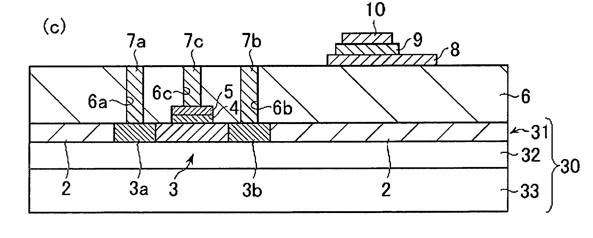
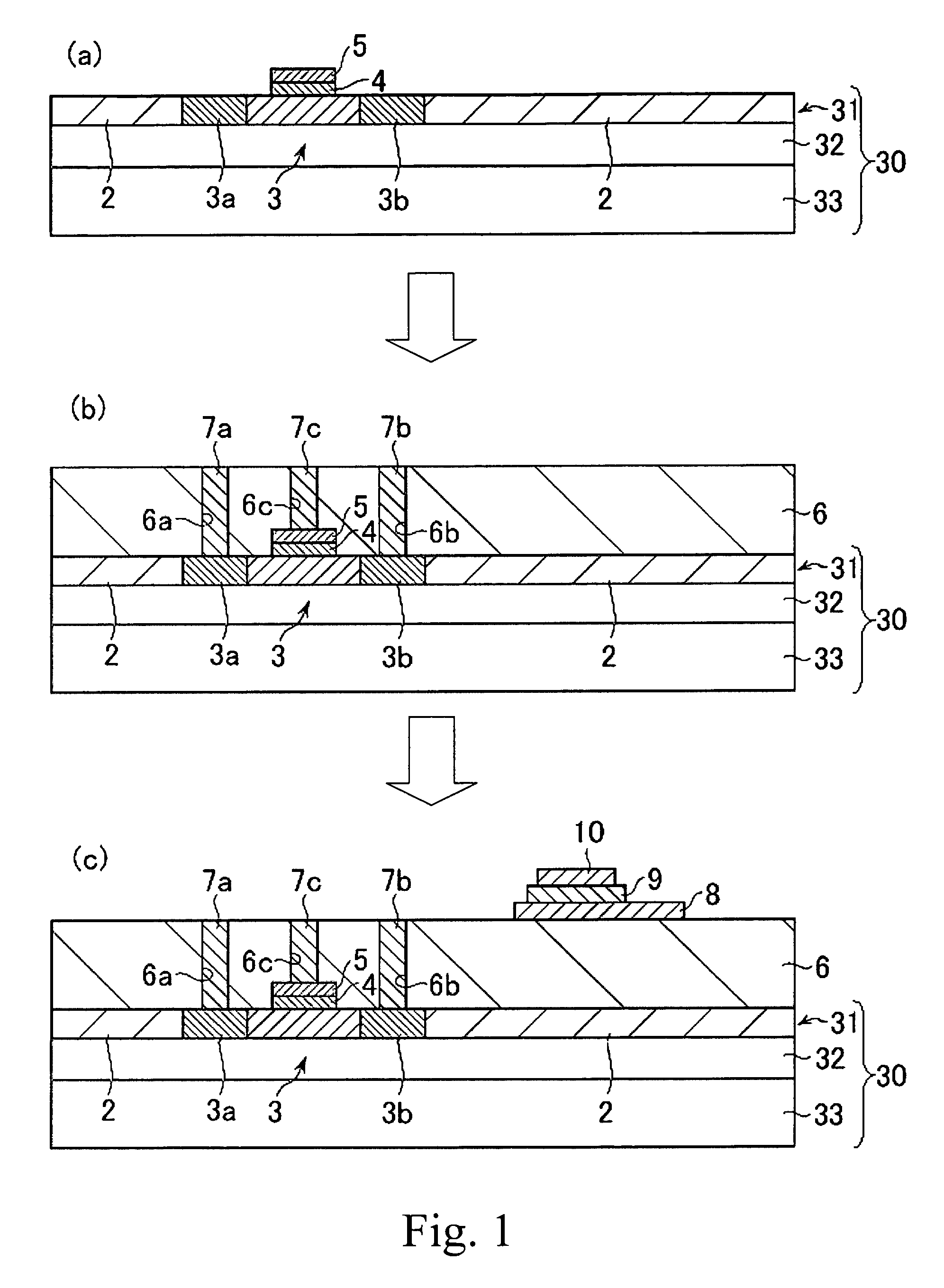
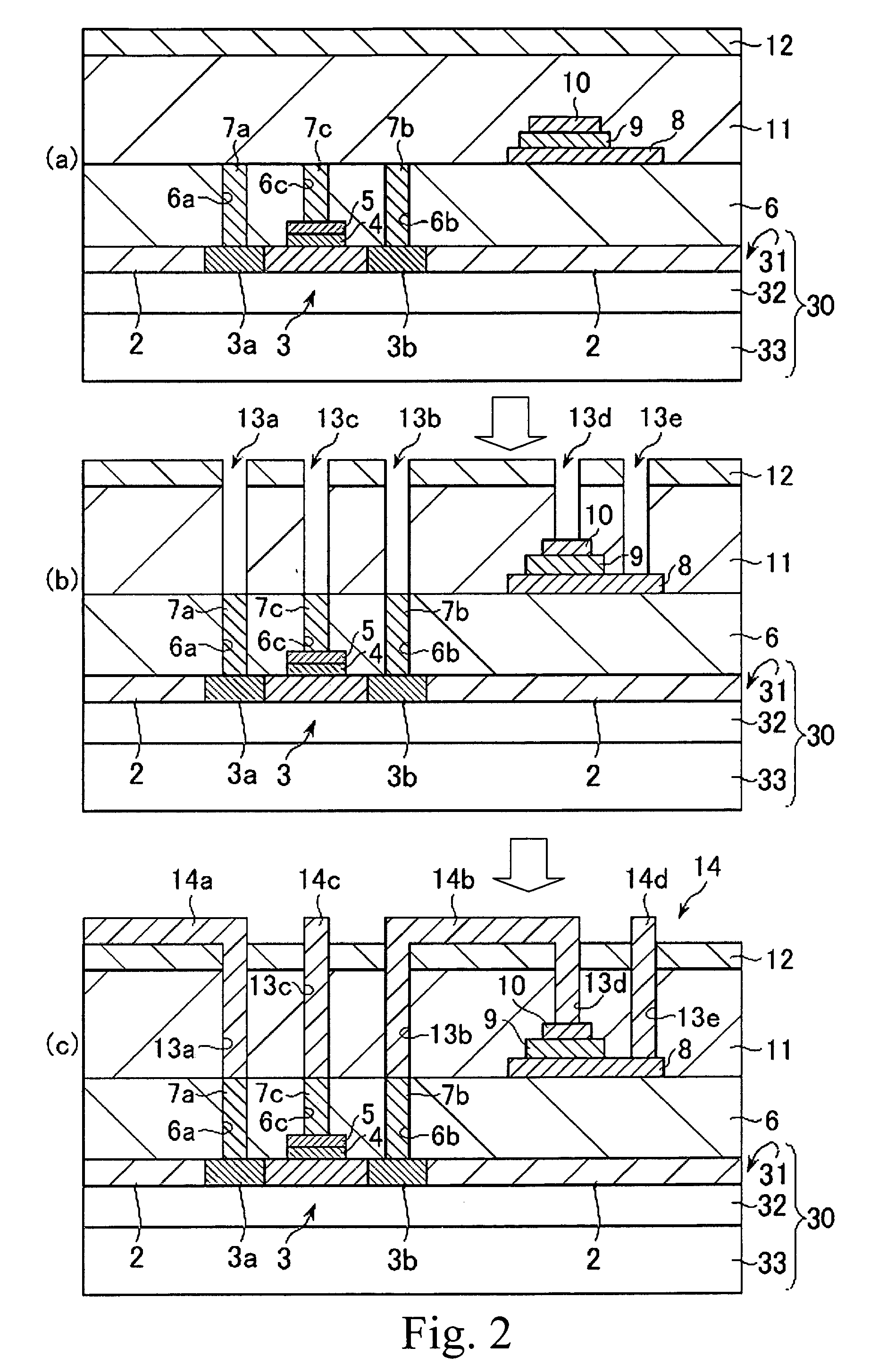
[0037] A second embodiment will now be explained. In view of the similarity between the first and second embodiments, the parts of the second embodiment that are identical to the parts of the first embodiment will be given the same reference numerals as the parts of the first embodiment. Moreover, the descriptions of the parts of the second embodiment that are identical to the parts of the first embodiment may be omitted for the sake of brevity.

[0038]FIG. 5 is a cross-section diagrammatical view of semiconductor device 1 in accordance with a second embodiment of the present invention. The semiconductor device 1 of the second embodiment is a ferroelectric memory device with a stack typed ferroelectric capacitor. The present embodiment is different from the first embodiment in that the lower electrode 8 of the ferroelectric capacitor is formed on the contact plug 7b, which is located in the interlayer insulating layer 6. That is, the lower electrode 8 of the ferroelectric capacitor h...


PUM


Abstract

A method of manufacturing a semiconductor device includes: forming a transistor with first and second ends 3a and 3b of a main current path, and a control electrode 5, covering the transistor with a first insulating film 6, forming first through third openings that expose the first and second ends 3a and 3b and the control electrode 5, and burying or filling first to third conductive materials 7a-7c in the first to third openings respectively, forming the ferroelectric capacitor by laminating the first electrode 8, the ferroelectric film 9, and the second electrode 10, laminating the second insulating film 11 and the moisture diffusion protective film 12, forming the fourth opening 13c to expose the third conductive material 7c through the second insulating film 11 and the moisture diffusion protective film 12, and forming a first wiring layer 14c, which has electrical connection with the control electrode 5.

Description

BACKGROUND OF THE INVENTION [0001] 1. Field of the Invention [0002] The present invention relates to a semiconductor device and a method of manufacturing the same. More specifically, the present invention relates to a semiconductor device with a ferroelectric capacitor and method of manufacturing the same. [0003] 2. Background Information [0004] Related examples of a semiconductor device with a ferroelectric capacitor are described in Japanese Patent Publications JP-A-2003-100994 and JP-A-1995-50391, which are hereby incorporated by reference. The former document describes a semiconductor device. Japanese Patent Publication JP-A-2003-100994 also discloses a semiconductor device that has a transistor, a ferroelectric capacitor, and a first wiring layer (1M). The transistor is formed on a semiconductor substrate. The ferroelectric capacitor is formed on a transistor via a first insulating layer. The first wiring layer (1M) is formed on the ferrolectric capacitor via a second insulatin...

Claims


Application Information

Patent Timeline
Patent Type & Authority Applications(United States)
IPC IPC(8): H01L21/8246H01L21/84H01L27/105H01L27/115H01L27/12
CPCH01L21/84H01L27/1203H01L27/11507H01L27/11502H10B53/30H10B53/00
Inventor TAKAYA, KOJI
Owner LAPIS SEMICON CO LTD
Why Eureka
Try Eureka