Bonded structures

a technology of bonded structures and adhesives, applied in the direction of soldering devices, instruments, photomechanical devices, etc., can solve the problems of other adhesives, such as solder, having other long-term reliability problems, and damage sensitive integrated devices

Active Publication Date: 2019-06-27
INVENSAS BONDING TECH INC
View PDF4 Cites 62 Cited by
  • Summary
  • Abstract
  • Description
  • Claims
  • Application Information

AI Technical Summary

Problems solved by technology

Moisture or some gases, such as hydrogen or oxygen gas, can damage sensitive integrated devices.
Other adhesives, such as solder, may have other long-term reliability issues.

Method used


Image

  • Bonded structures
  • Bonded structures
  • Bonded structures

Examples


Embodiment Construction

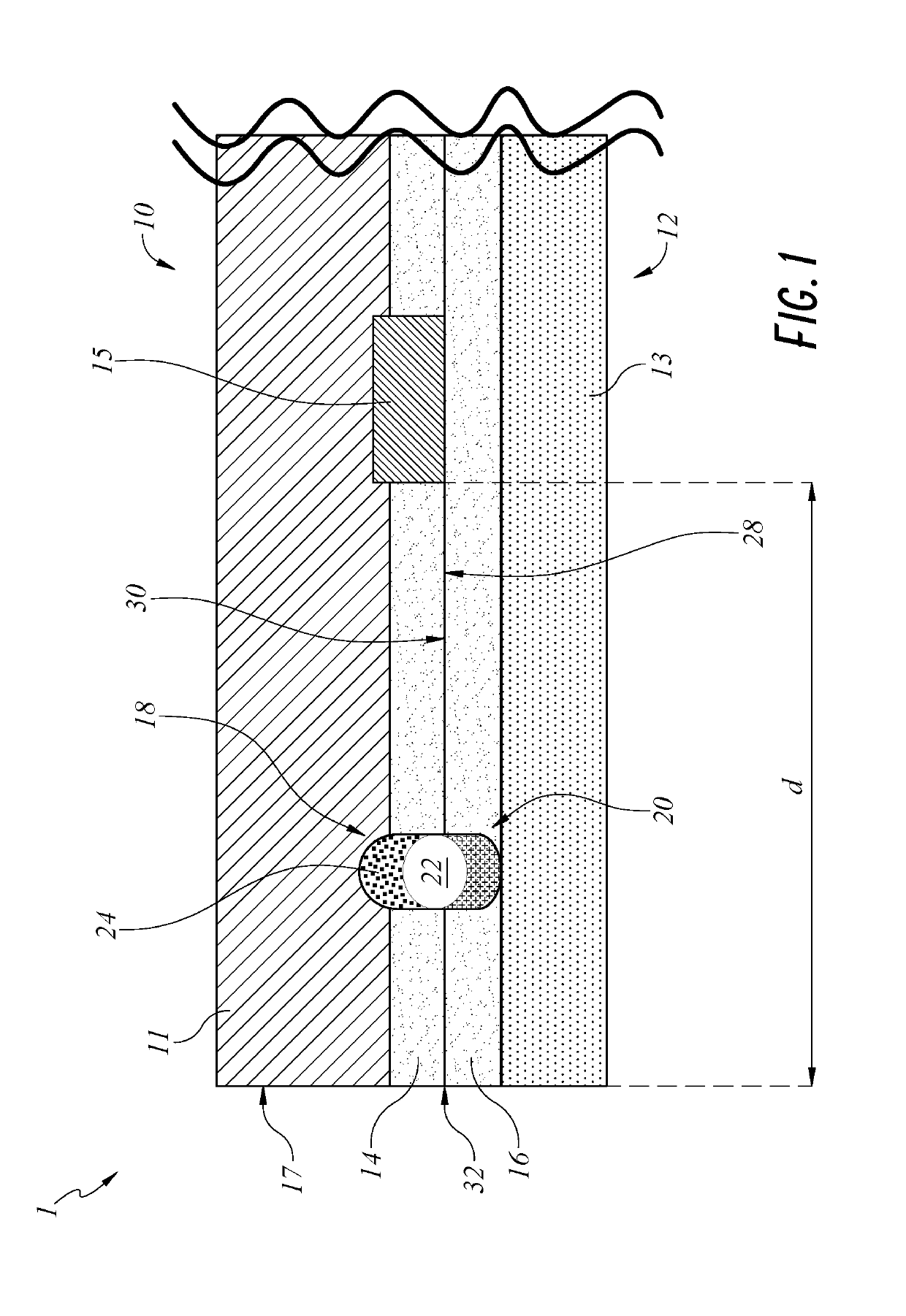
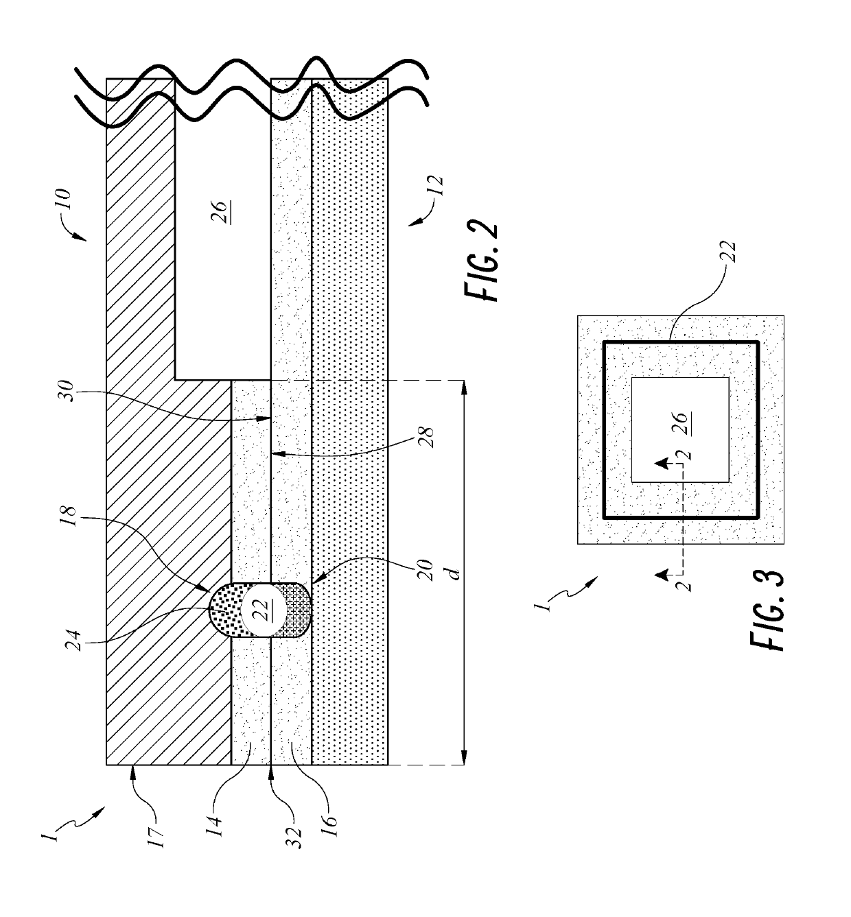
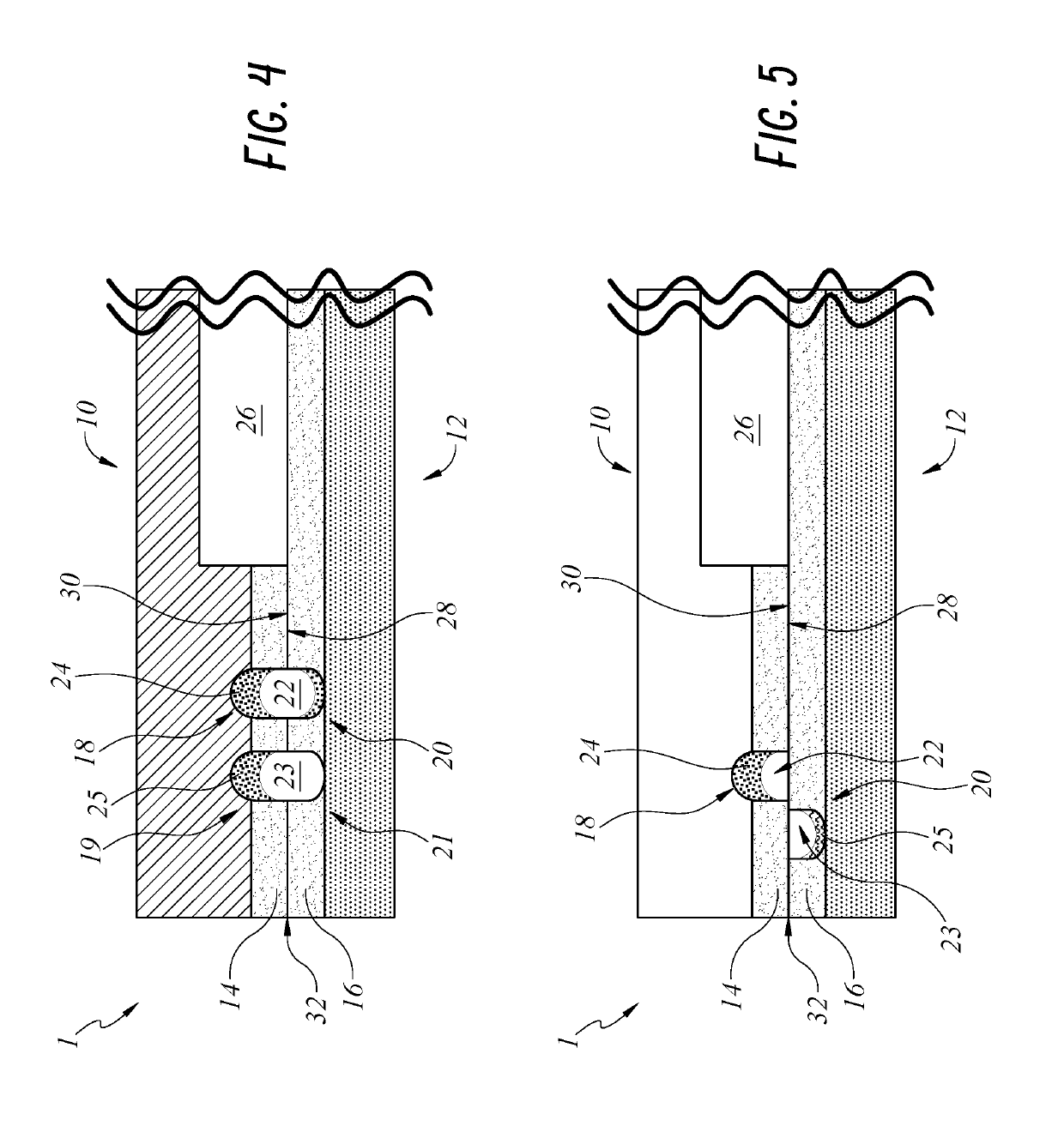
[0022]Various embodiments disclosed herein relate to bonded structures that connect two elements (which may comprise semiconductor elements) in a manner that effectively seals interior portions and / or integrated devices of the semiconductor elements from the outside environs. For example, in some embodiments, a bonded structure can comprise a plurality of semiconductor elements bonded to one another along a bonding interface. An integrated device can be coupled to or formed with a semiconductor element. For example, in some embodiments, the bonded structure can comprise a microelectromechanical systems (MEMS) device in which a cap (a first semiconductor element) is bonded to a carrier (a second semiconductor element). A MEMS element (the integrated device) can be disposed in a cavity defined at least in part by the cap and the carrier. In other embodiments, the element(s) can comprise other types of elements, such as optical elements, etc.

[0023]In some arrangements, the bonded struc...


PUM

PropertyMeasurementUnit
surface roughnessaaaaaaaaaa
degree of smoothnessaaaaaaaaaa
thicknessaaaaaaaaaa

Abstract

A bonded structure is disclosed. The bonded structure can include a first element that has a first bonding surface. The bonded structure can further include a second element that has a second bonding surface. The first and second bonding surfaces are bonded to one another along a bonding interface. The bonded structure can also include an integrated device that is coupled to or formed with the first element or the second element. The bonded structure can further include a channel that is disposed along the bonding interface around the integrated device to define an effectively closed profile The bonded structure can also include a getter material that is disposed in the channel. The getter material is configured to reduce the diffusion of gas into an interior region of the bonded structure.

Description

CROSS-REFERENCE TO RELATED APPLICATIONS[0001]This application claims the benefit of U.S. Provisional Application No. 62 / 609,683 entitled “BONDED STRUCTURES,” filed Dec. 22, 2017, the entire disclosure of which is incorporated herein by reference for all purposes.BACKGROUNDField[0002]The field generally relates to bonded structures, and in particular, to bonded structures having a getter material for sealing an internal portion of the bonded structures.Description of the Related Art[0003]In semiconductor device fabrication and packaging, some integrated devices are sealed from the outside environs in order to, e.g., reduce contamination or prevent damage to the integrated device. For example, some microelectromechanical systems (MEMS) devices include a cavity defined by a cap attached to a substrate with an adhesive such as solder. However, some adhesives may be permeable to gases, such that the gases can, over time, pass through the adhesive and into the cavity. Moisture or some gas...

Claims


Application Information

Patent Timeline
Patent Type & Authority Applications(United States)
IPC IPC(8): H01L23/26H01L21/322H01L23/10H01L23/00B81B7/00B81C3/00
CPCH01L23/26H01L21/3221H01L23/10H01L24/09H01L24/03B81B7/0038B81C3/001H01L23/04H01L2224/08145H01L2224/80011H01L24/80H01L2224/80896H01L2224/32145H01L2224/2919H01L2224/32225H01L2224/08225
Inventor KATKAR, RAJESHWANG, LIANG
Owner INVENSAS BONDING TECH INC
Why Eureka
Try Eureka