Die seal ring for integrated circuit system with stacked device wafers

a technology of integrated circuit system and die seal, which is applied in the direction of semiconductor/solid-state device details, radiation controlled devices, semiconductor devices, etc., can solve the problems of compromising the integrity and reliability of the integrated circuit, additional weakness at the bonding interface between the stacked wafers, and cracking at the die edg

Active Publication Date: 2014-05-08
OMNIVISION TECH INC
View PDF14 Cites 61 Cited by
  • Summary
  • Abstract
  • Description
  • Claims
  • Application Information

AI Technical Summary

Problems solved by technology

However, using a diamond saw introduces mechanical stress to the semiconductor wafer and can result in cracking at the die edge and compromising the integrity and reliability of the integrated circuit.
Furthermore, there is an additional weakness created at the bonding interface between the stacked wafers.

Method used


Image

  • Die seal ring for integrated circuit system with stacked device wafers
  • Die seal ring for integrated circuit system with stacked device wafers
  • Die seal ring for integrated circuit system with stacked device wafers

Examples


Embodiment Construction

[0015]Embodiments of a Die Seal Ring for Integrated Circuit System with Stacked Device Wafers are described herein. In the following description numerous specific details are set forth to provide a thorough understanding of the embodiments. One skilled in the relevant art will recognize, however, that the techniques described herein can be practiced without one or more of the specific details, or with other methods, components, materials, etc. In other instances, well-known structures, materials, or operations are not shown or described in detail to avoid obscuring certain aspects.

[0016]Reference throughout this specification to “one embodiment” or “an embodiment” means that a particular feature, structure, or characteristic described in connection with the embodiment is included in at least one embodiment of the present invention. Thus, the appearances of the phrases “in one embodiment” or “in an embodiment” in various places throughout this specification are not necessarily all re...


PUM


Abstract

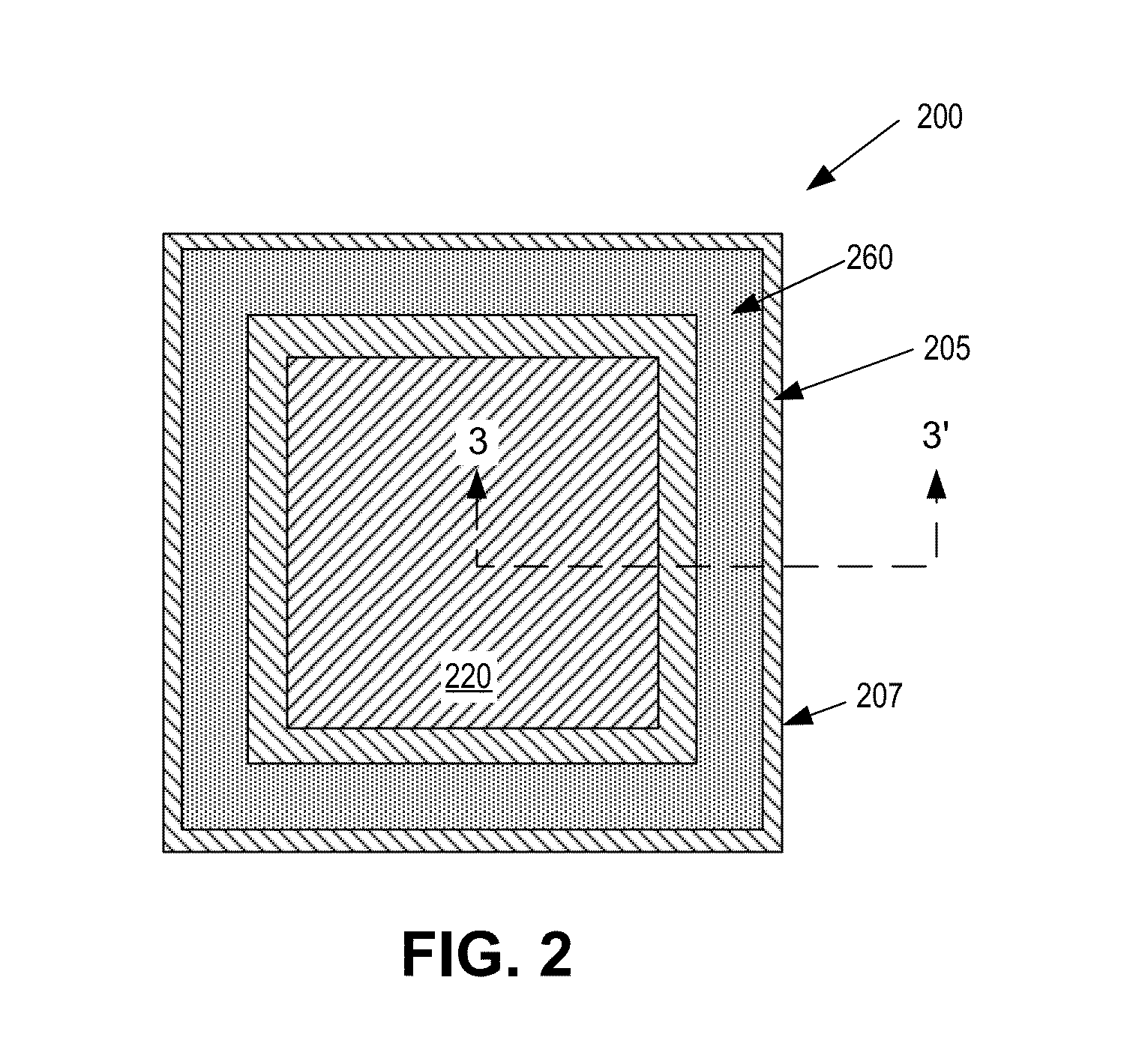
An integrated circuit system includes a first device wafer bonded to a second device wafer at a bonding interface of dielectrics. Each wafer includes a plurality of dies, where each die includes a device, a metal stack, and a seal ring that is formed at an edge region of the die. Seal rings included in dies of the second device wafer each include a first conductive path provided with metal formed in a first opening that extends from a backside of the second device wafer, through the second device wafer, and through the bonding interface to the seal ring of a corresponding die in the first device wafer.

Description

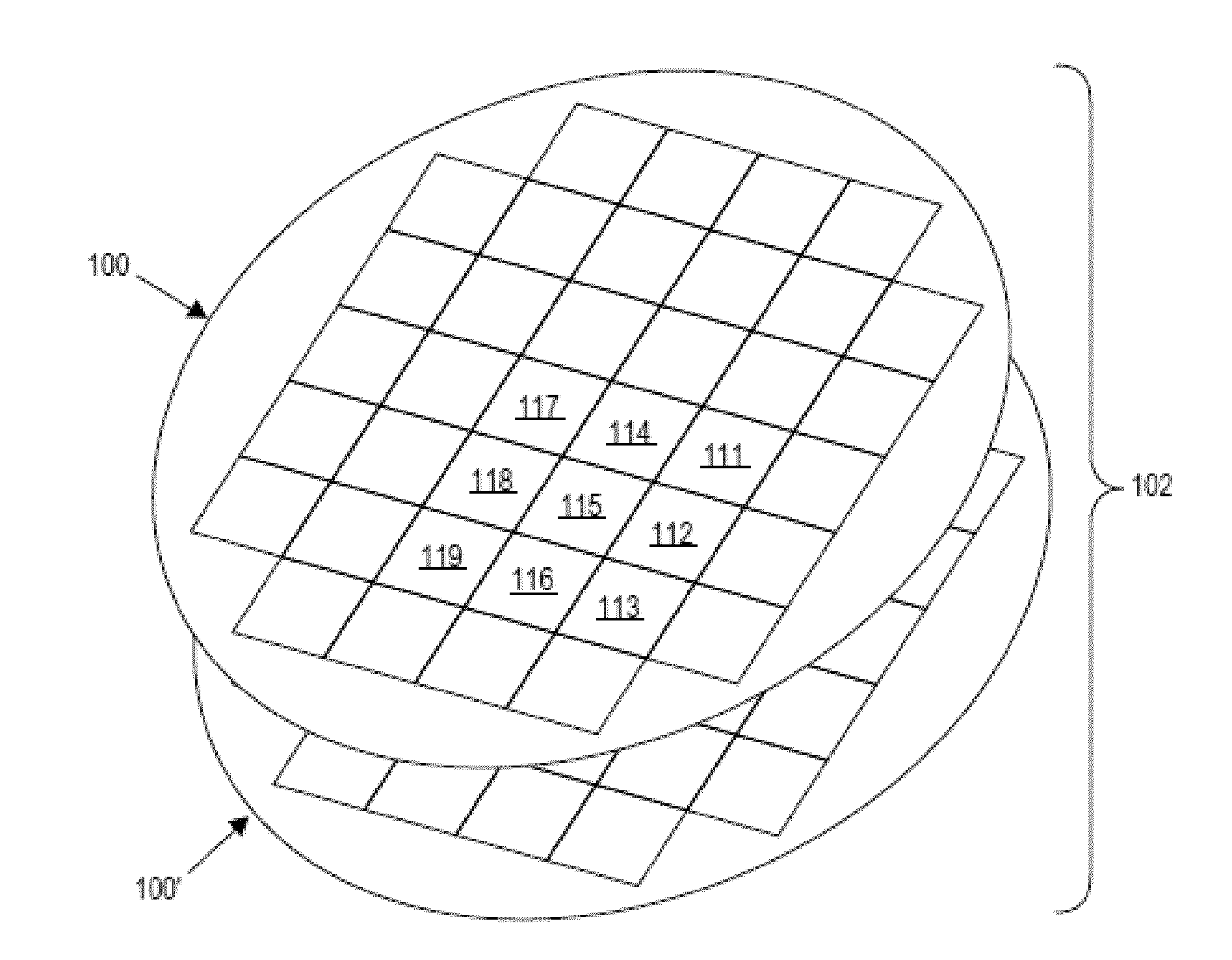
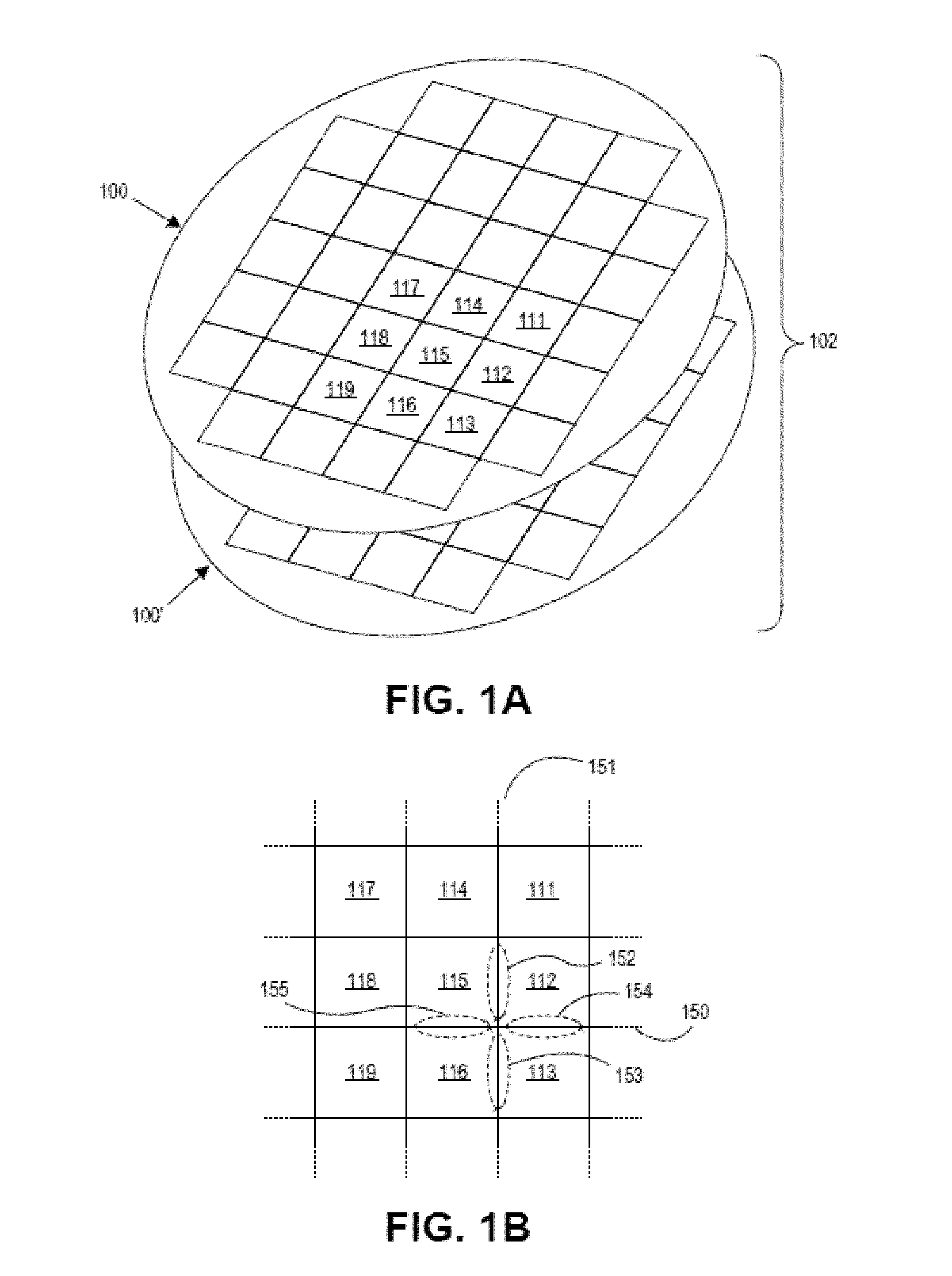
TECHNICAL FIELD[0001]This disclosure relates generally to semiconductor processing, and in particular but not exclusively, relates to semiconductor processing of stacked integrated circuit systems.BACKGROUND INFORMATION[0002]A semiconductor chip, or die (such as an image sensor chip) is fabricated on a single semiconductor wafer, along with hundreds and in some cases thousands of copies of the same die. Separating a semiconductor wafer into individual dies can be done with a die saw (such as a diamond saw). Cuts are made along areas of non-functional semiconductor material separating each die known as scribe lines. However, using a diamond saw introduces mechanical stress to the semiconductor wafer and can result in cracking at the die edge and compromising the integrity and reliability of the integrated circuit. One structure used to make a die less susceptible to the mechanical stress of die saws are seal rings. A die seal ring is formed in or on an outer edge region of one or mor...

Claims


Application Information

Patent Timeline
Patent Type & Authority Applications(United States)
IPC IPC(8): H01L27/146H01L21/30H01L31/18H01L23/52
CPCH01L27/14636H01L27/14683H01L2924/37001H01L23/585H01L24/05H01L24/08H01L24/94H01L2224/04042H01L2224/05567H01L2224/08145H01L2224/80896H01L2224/94H01L2924/10253H01L2924/10329H01L2924/1434H01L2224/9202H01L2924/00014H01L2924/12043H01L21/76898H01L23/481H01L27/1469H01L27/14689H01L27/14618H01L2224/9212H01L2224/80H01L2224/05552H01L2924/00H01L2224/8203H01L2224/821H01L2224/80001H01L2224/82
Inventor QIAN, YINTAI, HSIN-CHIHDAI, TIEJUNMAO, DULIYANG, CUNYURHODES, HOWARD E.
Owner OMNIVISION TECH INC
Why Eureka
Try Eureka