Methods for silicon-on-insulator (SOI) manufacturing with improved control and site thickness variations and improved bonding interface quality

a technology of silicon-on-insulator and manufacturing method, which is applied in the direction of semiconductor/solid-state device manufacturing, basic electric elements, electric apparatus, etc., can solve the problems of defect and delamination of the bonded region and interface, the probability of canceled defects being extremely low, and the typical non-reach of the goal

Inactive Publication Date: 2002-12-12
SILICON EVOLUTION
View PDF0 Cites 64 Cited by
  • Summary
  • Abstract
  • Description
  • Claims
  • Application Information

AI Technical Summary

Problems solved by technology

This is an idealized situation, which is typically not achieved in reality.
However, in wafer bonding for SOI, the irregularities will cause defects and delamination of the bonded region and interface.
Since almost all single side polished (SSP) wafers have such irregularities, the probability that these defects cancel each other is extremely low.
Consequently, the yield for such

Method used


Image

  • Methods for silicon-on-insulator (SOI) manufacturing with improved control and site thickness variations and improved bonding interface quality
  • Methods for silicon-on-insulator (SOI) manufacturing with improved control and site thickness variations and improved bonding interface quality
  • Methods for silicon-on-insulator (SOI) manufacturing with improved control and site thickness variations and improved bonding interface quality

Examples


Embodiment Construction

[0018] The ensuing description provides preferred exemplary embodiment(s) only, and is not intended to limit the scope, applicability or configuration of the invention. Rather, the ensuing description of the preferred exemplary embodiment(s) will provide those skilled in the art with an enabling description for implementing a preferred exemplary embodiment of the invention. It being understood that various changes may be made in the function and arrangement of elements without departing from the spirit and scope of the invention as set forth in the appended claims.

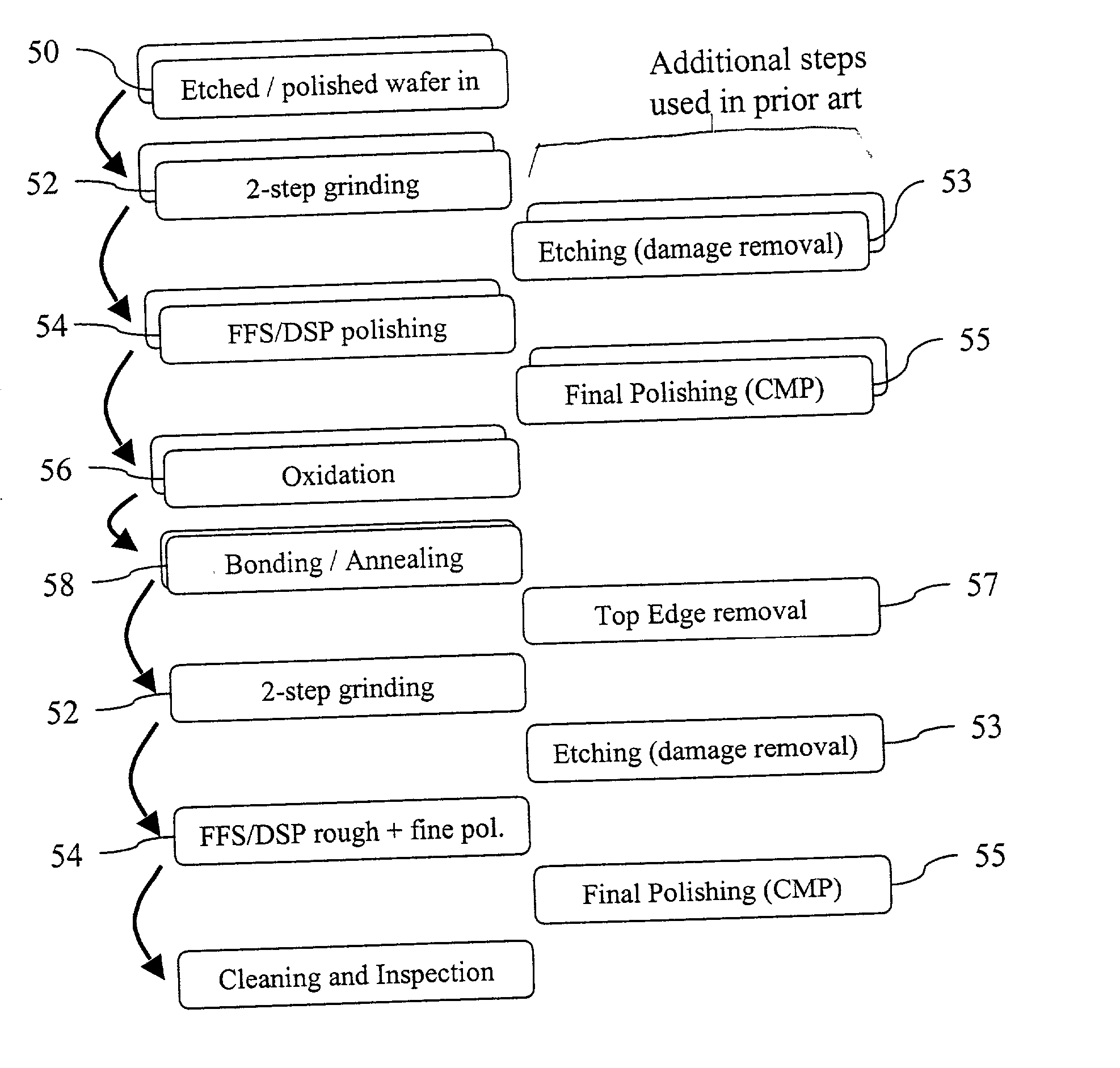
[0019] The present invention discloses a unique sequence of processing steps, one embodiment shown in FIG. 5, for the production of silicon-on-insulator (SOI) wafers. The invention provides wafer shapes as shown in FIG. 6 for illustration, resulting in improved layer interface quality and tighter control of the device layer thickness and properties than the other existing wafer bonding and wafer thinning processes, especia...


PUM


Abstract

A method for the production of silicon-on-insulator (SOI) wafers for controlling the device layer thickness variations and improvement of bonding quality at the interface of the wafers is disclosed. Using standard etched wafers, a unique sequence of process steps consisting of 2-step front side grinding, free-floating simultaneous double side polishing prepares wafers with low TTV and reduced edge roll off zones. The much smaller unbonded edge zone eliminates the requirements for edge grinding or etching in most cases. When the same s-step grinding/FFS-DSP sequence is applied after bonding and annealing of a Silicon-on-Insulator package, the resulting thickness variation in the device layer is usually smaller than what would be obtained from prior art processes.

Description

CROSS-REFERENCES TO RELATED APPLICATIONS[0001] This application claims priority to and incorporates by reference U.S. patent application Ser. No. 09 / 632,642 filed Aug.4, 2000, which claims priority to U.S. Provisional Application No. 60 / 147,432 filed Aug. 4, 1999.[0002] 1. Field of the Invention[0003] This invention relates generally to methods of production of silicon-on-insulator (SOI) wafers applicable to both thin and thick film processes. More particularly, the present invention pertains to an improved layer and interface quality especially close to the wafer's edge as well as a tighter control of device layer thickness and properties during wafer bonding and thinning processes.[0004] 2. Description of the Related Art[0005] Silicon-on-insulator (SOI) structures are of great importance in microelectronic device technologies. SOI structures may consist of a thick inactive base layer, typically but not necessarily made of silicon, that provides mechanical stability, an electricall...

Claims


Application Information

Patent Timeline
IPC IPC(8): H01L21/762
CPCH01L21/76256
Inventor WALITZKI, HANS J.DICHMANN, KURT U.MAGEE, THOMAS J.NICOLESCO, CLAUDIAN
Owner SILICON EVOLUTION
Why Eureka
Try Eureka