Display device, image display method and device, and light source module driving method and device.

A technology of display device and image data, applied in optics, nonlinear optics, static indicators, etc., to achieve the effect of reducing color separation effect, suppressing color separation, and improving refresh rate

Pending Publication Date: 2021-11-30
BOE TECH GRP CO LTD
0 Cites 0 Cited by

AI-Extracted Technical Summary

Problems solved by technology

[0005] Embodiments of the present disclosure provide a display device, a method and device for displaying images, and a driv...

Method used

[0096] In the display device of the embodiment of the present disclosure, the second flat layer 14 is provided on the side of the reflective layer 13 facing the second substrate 20, the second flat layer 14 can flatten the uneven surface of the reflective layer 13, and the multi- The first electrodes 15 are arranged on the surface of the second flat layer 14, so that the first electrodes 15 have a flat surface, which is conducive to the regular arrangement of liquid crystals and improves the display effect.
[0098] In one embodiment, the reflective layer 13 can be made of metal to increase reflectivity. The reflective layer 13 can shield the metal traces on the base substrate 11 and prevent the metal traces on the base substrate 11 from affecting the reflected light, which is beneficial to improve the aperture ratio of the display device. In the embodiments of the present disclosure, the aperture ratio of the display device can reach 85% to 95%.
[0099] In one embodiment, the reflective layer 13 may include a plurality of reflective blocks 131 separated from each other, and the plurality of reflective blocks 131 correspond to the plurality of first electrodes 15 one-to-one, and each reflective block 131 is connected to the base substrate 11. Corresponding thin film transistors are connected, and each first electrode 15 is connected to a corresponding reflective block 131 , for example, each first electrode 15 is connected to a corresponding reflective block 131 through a via hole passing through the second planar layer 14 . In this way, the first electrode 15 is avoided from being directly connected to the thin film transistor through the deeper via holes passing through the second flat layer 14, the reflective layer 13 and the raised structure layer 12, and the reflective block 131 is used as the first electrode 15 to connect with the thin film transistor. The transfer line connected to the thin film transistor has a relatively large area of ​​the reflective block 131 , which not only reduces the connection resistance between the first electrode 15 and the thin film transistor, but also simplifies the manufacturing process.
[0104] Exemplarily, in a pixel area, the orthographic projection boundaries of adjacent protrusions 121 on the base substrate 11 are in contact, as shown in FIGS. 4a and 4b. Therefore, more protrusions 121 can be provided in one pixel area, which can further increase the brightness of reflected light in the pixel area and improve the display effect.
[0125] FIG. 8 is a schematic diagram of the arrangement of a plurality of LEDs in a display device according to another embodiment of the present disclosure. As shown in Figure 8, multiple light-emitting diodes are divided into multiple LED light-emitting groups, and each of the R light-emitting diodes, G light-emitting diodes, and B light-emittin...

Abstract

The embodiment of the invention provides a display device, an image display method and device and a light source module driving method and device. The display device comprises a first substrate and a second substrate, wherein the first substrate comprises a substrate body, a protruding structure layer located on the side, facing the second substrate, of the substrate body, a reflecting layer located on the side, facing the second substrate, of the protruding structure layer, a second flat layer located on the side, facing the second substrate, of the reflecting layer, and a plurality of first electrodes located on the side, facing the second substrate, of the second flat layer and corresponding to the pixel areas in a one-to-one mode, wherein the protruding structure layer is provided with a plurality of projections, the surface of the reflecting layer is a concave-convex surface along with the plurality of projections, each first electrode is connected with a corresponding thin film transistor in the substrate body, and the reflecting layer is configured to reflect light rays incident from one side, deviating from the first substrate, of the second substrate. According to the technical scheme, flatness of the surface of the first electrode is guaranteed, regular arrangement of liquid crystals is facilitated, and the display effect is improved.

Application Domain

Static indicating devicesNon-linear optics

Technology Topic

Liquid crystallineLight source +8

Image

  • Display device, image display method and device, and light source module driving method and device.
  • Display device, image display method and device, and light source module driving method and device.
  • Display device, image display method and device, and light source module driving method and device.

Examples

  • Experimental program(1)

Example Embodiment

[0091] Hereinafter, some exemplary embodiments are simply described. As will be appreciated by those skilled in the art, the described embodiments can be modified in a variety of different ways without departing from the spirit or scope of the present disclosure. Thus, the drawings and descriptions are considered to be exemplary rather than restrictive.
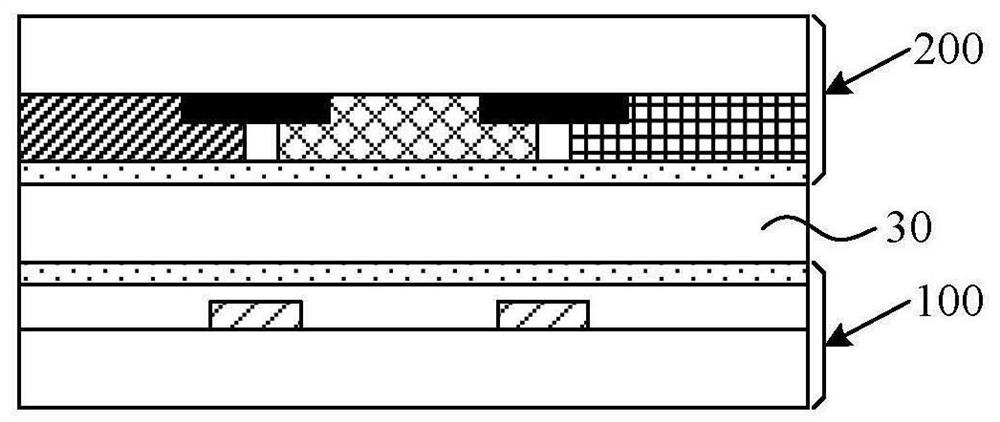
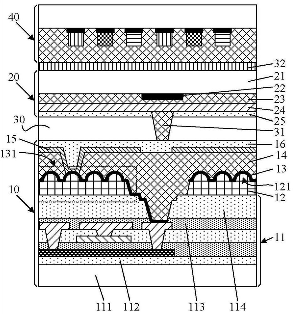
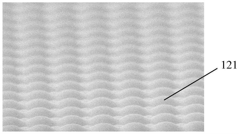
[0092] In the related art, in the reflective liquid crystal display device, the pixel electrode is formed on the uneven surface, resulting in unevenness of the pixel electrode surface, resulting in unregulating liquid crystal arrangement, affecting the display effect.
[0093] figure 2Schematic structural diagram of a display apparatus in an embodiment of the present disclosure. like figure 1 , The display device may include a first substrate 10 and second substrate 20 disposed opposite, further comprising a liquid crystal layer 30 located between the first substrate 20 and the second substrate 10. The display device may further include a light source module 40, the light source module 40 positioned at one side of the first substrate 10 away from the second substrate 20.
[0094] The first substrate 10 can also be called an array substrate, a first substrate 10 includes a plurality of pixel areas. like figure 2 , The first substrate 10 includes a base substrate 11, layer 12 toward the convex structure 20 side of the second substrate located on base substrate 11 between the convex structure layer toward the reflective layer 20 side of the second substrate 12 13, planarization layer 14 is located towards the second side of the second substrate 20 of the reflective layer 13, and a plurality of side 20 of the substrate 14 toward the second planar layer of the first electrode 15 second. The plurality of first electrodes 15 and the plurality of pixel regions correspond, the pixel corresponding to each region of the first electrode 15, each of the first electrode 15 is connected to the base substrate 11 corresponding to the thin film transistor. Wherein the raised structure 20 toward the surface layer side of the second substrate 121 is provided with a plurality of protrusions 12, such that the surface of the reflective layer 13 with a plurality of projections 121 form the surface irregularities. Reflective layer 13 is configured to reflect light from the second substrate 20 facing away from the side of the first substrate 10 is incident.
[0095] Embodiment of the present disclosure by the display device is a reflective display device, the light from the upper side of the second substrate 20 (the side facing away from the first substrate 10) by irradiating the liquid crystal layer is incident to the reflective layer 30 reflects 13, the reflective layer 13 reflected light 20 is emitted through the liquid crystal layer 30 and a second substrate, a display realized.
[0096] A display device according to embodiment of the present disclosure, the second planar layer is disposed on the side facing the reflective layer 13, 14 of the second substrate 20, a second planarization layer 14 may be uneven surface of the reflective layer 13 is planarized, a first plurality electrode 15 is provided on the planar surface of the second layer 14, so that the first electrode 15 has a flat surface, facilitate regular arrangement of liquid crystal, improve the display effect.
[0097] Illustratively, the first electrode 15 is a transparent electrode, the first electrode 15 may be called a pixel electrode, a liquid crystal deflection control. Material of the first electrode 15 may be a transparent conductive material such as indium tin oxide (ITO) or indium zinc oxide (IZO) and the like.
[0098] In one embodiment, the material of the reflective layer 13 may be a metal, in order to increase the reflectivity. The reflective metal layer 13 can block on the alignment base substrate 11, to avoid the metal on the base substrate 11 traces an impact on the reflected light, help to improve the aperture ratio of the display device. Example embodiments of the present disclosure display scale aperture ratio can reach 85-95%.
[0099] In one embodiment, the reflective layer 13 may include a plurality of block 131 reflecting off each other, a plurality of reflector block 131 correspond to the plurality of first electrodes 15, 11 of each reflector block 131 and the substrate corresponding to the substrate film transistors are connected, each of the first electrode 15 connected to the corresponding reflecting block 131, illustratively, via each of the first electrode 15 connected to the reflector by passing through the block 131 corresponding to the second layer 14 is planar. In this manner, avoiding the first electrode 1514, the reflective layer 13 and the deep hole through the thin film transistor layer 12 protruding structures direct connection through the second planar layer, a reflective block 131 as the first electrode 15 and the patch cord connected to the thin film transistor, a reflective block 131 larger, not only reduces the connection resistance between the first electrode 15 and the thin film transistor, and simplifies the manufacturing process.
[0100] Illustratively, the second planar layer of material 14 may be an organic material, such as a resin. Material convex structure layer 12 may be an organic material, such as a resin.
[0101] image 3 Embodiment of the present disclosure a structural layer is a schematic view of one pixel region in the projection example of the display apparatus. In one embodiment, if figure 2 with image 3 Shown, within each pixel region are disposed a plurality of protrusions 121. Accordingly, the reflective layer 13 has an uneven surface in the pixel region. Such an arrangement can improve the reflected light intensity of each pixel region, help improve the display effect.
[0102] Figure 4A A plurality of protrusions in the present disclosure means a schematic arrangement of an embodiment example of the display, Figure 4B In the present disclosure means a plurality of protrusions arranged a schematic diagram of another embodiment of a display. In one embodiment, in one pixel region, three adjacent triangular projections 121 are arranged, such as Figure 4A Indicated. In one embodiment, in one pixel region, a plurality of projections arranged in array 121, such as Figure 4B.
[0103] In one embodiment, in one pixel region, two projections adjacent distance between the centers of 0.5μm to 121 of 20 m (inclusive).
[0104] Illustratively, in one pixel region, adjacent the boundary orthogonal projection of the projection 121 on the base substrate 11 in contact, such as Figure 4A with Figure 4B Indicated. Thus, in a pixel region more projections 121 may be provided to further enhance the brightness of the reflected light of the pixel region, to improve the display effect.
[0105] Illustratively, the projection 121 of the cross section (cross section parallel to the direction of the substrate 11 relative to the substrate) may be any shape of a polygonal shape, circular, etc. Bank angle projections 121 can range from 30 ° ~ 60 ° (inclusive). This raised structure 121 can improve the reflection effect of the surface, to improve the brightness of the display device.
[0106] In one embodiment, if figure 2 , The base substrate 11 includes a first substrate 111, the first substrate 111 positioned toward the second substrate 20 side of the buffer layer 112, a buffer layer 20 toward the thin film transistor of the second substrate 112 side. The thin film transistor may be a bottom gate thin film transistor or a top gate type thin film transistor. A thin film transistor active material layer may be one of an amorphous silicon (a-Si), low temperature polysilicon (LTPS), low-temperature polysilicon oxide (LTPO), oxides (Oxide) and the like. Base substrate 11 may further include a dielectric layer 113 located toward the second substrate 20 side of the thin film transistor, the dielectric layer 113 can also be called a passivation layer for protecting the thin film transistor. Base substrate 11 may further include a dielectric layer 113 toward the first planar layer 114 of the second substrate 20 side, a first planar layer 114 is a thin film transistor for a flat section and the circuit configuration of the difference resulting structure. Convex structure layer 12 is disposed on the first planar layer 114.
[0107] In one embodiment, the first substrate 10 may further include a first alignment layer 16, a first alignment layer 16 at the side facing the liquid crystal layer 15 of the plurality of first electrodes 30.
[0108] Figure 5 Example embodiments of the present disclosure a structural schematic top view of the base substrate in a display device. In one embodiment, if Figure 5 , The first substrate 10 includes a first direction along a plurality of gate lines Gate X and extending in the plurality of data lines extending in a second direction Y Data. A plurality of gate lines Gate, each of the two adjacent gate lines simultaneously transmitted on signal to the thin film transistor in the two rows of pixels simultaneously turned. Data in the plurality of data lines, each adjacent two data lines Data transmit data simultaneously so that data is written simultaneously to two rows of pixels.
[0109] In this manner, the refresh rate of the display device can be improved. For example, Figure 5 In the display process, the two simultaneously transmitted on signal Gate1, Datal and Data2 simultaneous transmission of data, with the data signal is written, two rows of pixels corresponding to two Gate1 open simultaneously. The number of physical lines 240 acts embodiment, the number is displayed as the refresh row signal line 120, to enhance the refresh rate.
[0110] In one embodiment, if figure 2 , The second substrate 20 includes a second substrate 21, located in the second substrate 30 facing the liquid crystal layer 21 of black matrix 22, the black matrix is ​​positioned toward the third planar layer 2322 of the liquid crystal layer 30 side. Illustratively, the second substrate 20 may further comprise a third planar layer 23 toward the second electrode layer 30 side of the liquid crystal layer 24, and a second alignment layer 30 toward the side of the liquid crystal layer of the second electrode layer 24 25.
[0111] Illustratively, the display device may be employed TN (Twist Nematic, twisted nematic) mode, VA (VerticalAlignment, vertical alignment) mode, ADS (Advanced Super Dimension Switch, Advanced Super Dimensional Switching) mode or IPS (In-Plane Switching, plane switching) mode. To achieve quick response, the thickness of the liquid crystal layer 30 may be 1.0um ~ 2.0um (inclusive). Illustratively, the display device of TN mode, the friction (Rubbing) in the direction of the second alignment layer 25 is 50 ° ~ 60 °, the rubbing direction of the first alignment layer 16 is 110 ° ~ 120 °.
[0112] In one embodiment, the display apparatus may further include a first substrate 10 and the support posts 20 between the second substrate 31, the support post 31 ensures that the cell gap of the liquid crystal layer, the thickness range of the support column 31 may be 1μm ~ 2μm (inclusive). Support posts 31 may be formed on the first substrate 10, or, the support posts 31 may be formed on the second substrate 20.
[0113] In one embodiment, the display apparatus may further include a circular polarizer 10 side of the first substrate 20 is positioned away from the second substrate 32, so that the incident light into circularly polarized light enters the liquid crystal layer 30. Circular polarizer 32 may include a linear polarizer stack disposed, quarter-wave plate and a half-wave plate.
[0114] In one embodiment, if figure 2 , The display device may further include a light source module 40, the light source module 40 is positioned away from the side of the first substrate 10 second substrate 20, that is, the light source module 40 located on the display side of the display device. 40 is a front light source module, the light source module 40 can emit light, the light passes through the reflective layer may be a light source module 40, the display achieved.
[0115] Image 6 Example embodiments of the present disclosure a schematic structural diagram of a display device of a light source module. In one embodiment, if Image 6 , The light source 40 may include a drive module 41 and a back plate disposed in a plurality of LED driving back plate 20 toward the side of the second substrate 41 (LED) 42. Illustratively, a first plurality of light emitting diodes may include color light emitting diodes, light emitting diodes of the second color and the third color light emitting diode. The first color, second and third colors may respectively R, G and B.
[0116] like Image 6 , The light source module 40 can further include a plurality of light-shielding layer 43 and the filling layer 44. A plurality of light shielding layers 43 and the plurality of light emitting diodes to-one correspondence. The light-shielding layer 43 is positioned between the light emitting diode 42 and the driver 41 backplane. Filling layer 44 on one side of the backing plate 41 toward the light emitting diode driver 42, and filled between the adjacent light emitting diode 42.
[0117] With this configuration, the light-shielding layer 43 can block the light leakage corresponding LED laterally, avoiding the light from the LED driving back plate 41 side exit, such that the LED light only toward the second substrate 20 side exit.
[0118] Illustratively, the surface of the backing plate 41 away from the drive side of the filler layer 44 and the back plate drive is greater than a distance between the light emitting diode 41 a distance between the driving surface 41 of backing plate 41 away from the drive side of the backing plate 42, That is, the light emitting diode 42 is located inside the filling layer 44, such asImage 6 As shown, the LED is completely covered in the filler layer 44. The filling layer 44 can reduce the reflection between the interface and protect the LED. The refractive index of the filler layer 44 is from 1.4 to 1.8 (including endpoint values), exemplarily, the refractive index of the fill layer 44 can be any value in 1.4 to 1.8. The material of the filler layer 44 can be selected as needed, as long as the refractive index of the filler layer 44 satisfies from 1.4 to 1.8.
[0119] like Image 6 As shown, the light-emitting diode 42 is in the plane parallel to the plane of the drive back plate 41 is W 1 The height of the light emitting diode 42 is h 1 The light shielding layer 43 is in the size parallel to the plane of the drive back plate 41. 2 The thickness of the light shielding layer 43 is h 2 The refractive index of the filler layer 44 is N, which satisfies the following relationship:
[0120] (W 2 / 2-w 1 / 2) / (h 1 + H 2 ) = TAN (arcsin (1 / n)).
[0121] Exemplarily, W 2 ≥2 * Tan (arcsin (1 / n)) * (h 1 + H 2 + W 1. For example, W 1 5μm, h 1 1μm, H 2 1μm, then w 2 More than or equal to 6.81 μm.
[0122] In one embodiment, the LED may be 5 μm * 5 μm to 30 μm * 30 μm in the plane parallel to the driving back plate 41.
[0123] Figure 7 Four arrangements for multiple LEDs. Exemplalily, multiple LEDs can be arranged in array, and the distance between the two LEDs can be the same, such as Figure 7 The middle (a) is shown. Exemplarily, R, G, B can be equally spaced, such as Figure 7 The middle (b) is shown.
[0124] In one embodiment, if Figure 7 In the middle (c), R, G, and B can be arranged in triangulation. In one embodiment, the plurality of light emitting diodes can be arranged in a set of four LEDs, and 4 LEDs in each group are RGBG, such as Figure 7 The middle (d) is shown.
[0125] Figure 8 A schematic diagram of a plurality of LEDs in the apparatus for the present disclosure. like Figure 8 As shown, the plurality of light emitting diodes are divided into a plurality of LED luminescence groups, which form an LED lighting group together with each R-light-emitting diode, a B-light-emitting diode, and a plurality of LED lighting groups are array. Rubber. This approach can improve the uniformity of the luminescence.
[0126] Illustratively, each LED can control the illumination of the plurality of pixel regions, the number of LEDs and the number of pixels may be 1: 5 to 1: 100. That is, each LED can control light emission of 5 to 100 pixels. In the case of R, g, b Binding (Bonding), together with an LED luminescence group, the number of LED lighting groups and the number of pixels may be 1: 5 to 1: 100. That is, each LED lighting group can control light emission of 5 to 100 pixels.
[0127] The present disclosure also provides a method of displaying an image, applied to the graph source processing module, which includes:
[0128] S210, according to the display device determines the resolution of the image data of the subframe picture to be displayed, the display resolution of the display device is smaller than the display resolution corresponding to the processing module of the graph source processing module;
[0129] S220, the image data of each subframe picture of each subframe picture of the display image is reconstituted according to the resolution of the image data of the image data of the subframe screen, and the image data to which each subframe picture of the display image is reconstituted, and the reconstruction of each subframe screen is obtained. Image data, the row resolution of the reconstructed image data is the same as the row resolution of the canable data of the graphical processing module;
[0130] S230, according to the resolution of the processing module of the graphic processing module, data fusion after the reconstruction of each subframe picture of the image to be displayed, and obtains corresponding to the fusion image data. Synthetic pictures, the resolution of the synthetic picture is the same as the display resolution corresponding to the processable data of the graphical processing module;
[0131] S240, transmitting image data of the synthetic picture to the display device from the illustration source processing module to display the image to be displayed by the display device.
[0132] Illustratively, the display device may employ a display device in the embodiment of the present disclosure, and the display device includes a plurality of pixels, but each pixel is no longer distinguished. The data voltage is used to achieve grayscale, the color of the display device is implemented by the LED lamp of different colors in the light source module. The graphical source processing module can include a plurality of pixels, each pixel can include a plurality of sub-pixels, such as three sub-pixels, respectively R sub-pixels, G sub-pixels, and B pixels.
[0133] It should be noted that the resolution of the image or picture is p * q, indicating that the row resolution is p, and each row has P pixels; the column resolution is Q, each column has q pixels. The resolution of the data is p * q, indicating that the row resolution is p, and each line has P data; the column resolution is Q, each column has Q data.
[0134] Exemplarily, an image is displayed, such as a color image, typically comprising three subframe screens, such as R subframe screen, G subframe screen, and B frame screen, such as Figure 9 Distance Figure 9 A schematic diagram of subframe screen decomposition for the image to be displayed. The resolution of the subframe screen is the same as the resolution of the image to be displayed. When the display device is scanned by a row of data, a column data transmission, when the display device displays the subframe screen, the resolution of the image data is the same as the display device of the display device. It should be noted that the resolution of the image data can also be called a signal input resolution.
[0135] For example, the resolution of the image to be displayed is 240 * 360, then each subframe screen has a resolution of 240 * 360. In the case of a row of data scanning, one column data transmission, the resolution of the image data of the subframe screen is 240 * 360, that is, 360 data per line, each column has 240 pieces. data. When the display device employs the display device in the embodiment of the present disclosure, the two data lines in the display device simultaneously transmit data, and the two gate lines simultaneously transmit the open signal, so that the resolution of the image data of the subframe screen is 120 * 720.
[0136] It should be noted that the map source processing module is used to process the data, and the graphical source processing module can be a separate module, or a data processing module in a display device. The display resolution corresponding to the processing module of the map source processing module is connected to the map source processing module and the display panel, the resolution of the display panel displayed.
[0137] Illustratively, in order to improve the image refresh rate, the display resolution of the display device is smaller than the display resolution corresponding to the canable data of the graph source processing module, that is, the display resolution of the display device is smaller than the graph source processing module. The display resolution of the display resolution may be handled, and the display resolution of the display device is smaller than the column resolution of the display resolution corresponding to the processing module of the graph source processing module. It will be appreciated that the display resolution of the display device is the resolution of the image that the display device can display, in the case of another display device, the display resolution of the icon source processing module is the icon source processing module. The resolution of the image that can be displayed. For images or images, the line resolution is the number of pixels per row, the column resolution is the number of pixels per column.
[0138] According to the related art, by increasing the refresh rate, reducing the color saturation of the light source and reduces brightness, the color separation can be reduced, but the color saturation can result in poor display effect, and the way to reduce the brightness cannot show a good picture effect. .
[0139] The method of displaying the display image of the present disclosure, by reconstructing the image data of each subframe picture of the display image, according to the resolution of the processing module, the number of images to be displayed, the number of images to be displayed is displayed. The reconstructed image data corresponding to the frame screen performs data fusion, obtains the same picture corresponding to the fused image data, the resolution of the synthetic picture is the same as the display resolution corresponding to the processing module of the graphical processing module, thereby The image data of the synthetic picture can be transmitted from the source processing module to the display device to display the image to be displayed by the display device. Since the display resolution of the display device is smaller than the display resolution corresponding to the canable data corresponding to the graphical processing module, the image data of the synthetic picture corresponds to the image data of the predetermined number, thereby transmitting the image data of the synthetic picture to When the display device is displayed, when the image data of the graphical source processing module refreshes the image data of the composite picture, the display device can refresh the predetermined amount of the image to be displayed, improve the refresh rate of the display device, and achieve the effect of suppressing color separation.
[0140] In one embodiment, step S230 can include: sequentially arranging the reconstructed image data corresponding to each subframe screen of the predetermined amount, obtaining the arrangement corresponding to the predetermined amount. The image data, the row resolution of the arranged image data is the same as the row resolution of the image data corresponding to each subframe screen; the resolution of the processing module according to the graphical source processing module, the arranged image Data synthesis, obtain the synthetic picture, the resolution of the synthetic picture is the same as the display resolution corresponding to the processing data of the graphical processing module.
[0141] Illustratively, the reconstruction of the preset number of the subframe screens corresponding to each subframe screen to be displayed in order can be arranged in order to display a subframe screen of different colors at time of time. For example, the first color subframe screen, the second color subframe screen, the third color subframe screen is displayed, so that the predetermined amount of the image is displayed.
[0142] In one embodiment, the image data of each subframe picture of each subframe screen to which the image is displayed according to the resolution of the resolution of the image data of the subframe screen and the resolution of the image source processing module, and each subframe screen is obtained. The corresponding reconstructed image data may include reconstructing each I row data in the image data of each subframe picture into a row of data, each subframe screen includes j row data, j is an integer multiple of I; After the reconstruction of the subframe screen, the row resolution of the reconstructed image data is the same as the row resolution of the canable data of the graphics process module, and the number of rows of image data after the reconstruction is j I.
[0143] Exemplarily, the display resolution corresponding to the processing data of the map source processing module is 1920 * 1080. Taking the R subframe screen as an example, the resolution of the R subframe screen (ie, the display resolution) is 240 * 360. The resolution of image data of the R subframe screen is 120 * 720, using the display device in the present disclosure. Figure 10 Distance Figure 10 A resolution schematic diagram of the image data of the R subframe picture in an embodiment of the present disclosure.
[0144]The resolution of the image data of the sub-frames, each sub-image data of 8 rows of data frames in a row of data is reconstructed. For example, i is set to 8, the sub-frame picture image data R from the data line 120 is below the upper, i.e. j = 120, the amount of data of each line is 720, the line 120 1 8 ~ line data, ~ 9 16 rows, ..., 113 to 120 lines of a row of data is reconstructed, reconstructed resolution of the image data is 15 * 5760, i.e., the reconstructed image data to data line 15, each row having data 5760, such as Figure 11 Distance Figure 11 A schematic view of an embodiment of the present disclosure reconstructed image data of Examples. Line resolution of the image data is reconstructed 5760, FIG display resolution processing module source line resolution of 1920, k is 3 (k is a number indicating the source channel processing module, i.e., the processing module for the source of FIG. number of channels for transmitting data). Incidentally, the channel number k indicating the source is not limited to the processing module 3 may also be other values. FIG source processing module can process data corresponding to the display resolution of the source line in FIG resolution processing module can process data resolution divided by the number of channels of row k.
[0145] It will be appreciated that the specific values ​​of i rows may require a processing module for processing data determined in accordance with the resolution of the resolution of the row of sub-frame picture image data and FIG source, so that the sub-frame picture corresponding to the image data reconstructed resolution resolution same row line in FIG source processing modules may process data, i.e., the line resolution of the image corresponding to the sub-frame picture reconstructed data processing module of FIG source line resolution display resolution k times better.
[0146] In one embodiment, the image to be displayed comprising a first sub-frames, the second and third sub-sub-frame picture frames, the preset number of images to be displayed after the screen data corresponding to the reconstructed image for each sub-frame in order of priority, to be obtained with a preset number of display image data corresponding to the image arrangement, may include: for each sub-image to be displayed after the image data corresponding to frame picture reconstructed in order of priority, to obtain a weight corresponding to the image to be displayed after configuration of the image data, the resolution of the image to be displayed in the same row after row after the resolution of an image corresponding to the image data reconstructed picture corresponding to each sub-frame reconstruction data, wherein the image to be displayed in the corresponding reconstructed after the image data, the image data corresponding to the picture reconstructed after each subframe the number of repetitions is m, m nonpositive integer 0; and the preset number of images to be displayed corresponding to the image data reconstructed in order of priority obtained with a preset number of images to be displayed relative to the image data corresponding to the arrangement, the line resolution of the image data to be displayed arranged in the same row of the resolution of the image data corresponding to the image reconstruction.
[0147] Illustratively, the need to obtain the image data to be displayed corresponding to the reconstructed image, since the images to be displayed comprising a first sub-frames, the second and third sub-sub-frame picture frames, whereby each of the image to be displayed sequentially arranged reconstructed image data corresponding to the sub-frames, it is possible to obtain the image data to be displayed corresponding to the image reconstruction. For example, the display image data to be reconstructed image comprises image data are sequentially arranged in a first sub-frame corresponding to the picture reconstruction, image data corresponding to the second sub-frame picture and the reconstructed picture corresponding to the third sub-frame the reconstructed image data. Each sub-frame picture corresponding to the regular arrangement of the reconstructed image data is to keep the resolution of the same row, so that, after the resolution of the image line corresponding to the image data to be displayed reconstructed picture corresponding to each sub-frame reconstructed after the same line-resolution image data.
[0148] The preset number of images to be displayed corresponding to the image data reconstructed in order of priority can be obtained with a predetermined number of image data to be displayed corresponding to the arrangement of the image. A preset number to be displayed after the arrangement rule reconstructed image data corresponding to the image resolution is kept constant line, so that, after the resolution of the image row array data to be displayed after an image corresponding to image data reconstructed resolution in the same row and the same line after the resolution of the image corresponding to the picture data to the sub-frame reconstructed.
[0149] For example, the preset number is 16, then the first sub-frames, a second number of sub-frames, and the third sub-frames are 16. The first sub frames may be sub-frames R, G second sub-frames may be sub-frames, the third sub-frames may be B sub-frames. Figure 12 A schematic view of the present disclosure according to the image data arranged in embodiments, such as Figure 12 FIG, m = 1, i.e. until the image data corresponding to the image reconstruction display, the image data corresponding to the R sub-frame picture reconstructed, image data corresponding to the G sub-frames, and B sub reconstructed frame picture corresponding to the image data reconstructed are a number of repetitions. The order of priority, obtaining an image to be displayed corresponding to the reconstructed image data after the image data corresponding to the R sub-frame picture reconstructed, G sub-frame picture image data corresponding to the B sub-frame and the reconstructed picture corresponding reconstructed after the image data, the image data corresponding to a display image to be reconstructed is 15 * 3 = 45 rows; the group 16 to be displayed after an image corresponding to image data reconstructed in order of priority, and the image data obtained after the arrangement, the arrangement after the image data is 45 * 16 rows. therefore, Figure 12 Image data arrangement shown is 15 * 3 * 16 = 720 rows, each row having 5760 data. Such arrangement, consistent with the principles of the field sequential display, displays in different colors to facilitate the sharing of sub-frames.
[0150] In one embodiment, the process according to the resolution FIG source module may process data, the image data of the arranged data synthesis, obtaining the synthetic image, may include: image data are stored in the arranged source processing module of FIG. k in the channel; fed into a plurality of rows of data into the virtual channel k, obtained with a preset number of images to be displayed corresponding to the synthetic image, the resolution of the source of FIG processing module may process the synthesized image data corresponding to a display the same resolution.
[0151] Illustratively, each of the source pixel map processing module includes an R subpixel, G subpixel, and B sub-pixels, and therefore, the number of the channel processing module of FIG source 3, i.e., k = 3, that is to say, the processing source module of FIG. there are three data transmission channels. Each line image data are arranged after the 5760 data, the data 5760 are stored in the three kinds of channels, each channel may be stored 5760/3 = 1920 data, as Figure 13 Distance Figure 13 A schematic diagram of a synthesized image in the embodiment disclosed. The number of rows of image data remains unchanged, thus holding the number of lines is 720 lines.
[0152] FIG source processing module can process data corresponding to a display resolution of 1920 * 1080, in order to make the data format of the source data format of FIG composite image processing module matches, can make up the multi-line virtual (dummy) data. Figure 13 You can complement the dummy data line 360, such as Figure 13 Shown, so as to obtain the image to be displayed corresponding to the composite image, the composite image is a full high definition (FHD) image, the composite image resolution of 1920 * 1080, the same processing module and the data processing corresponding to FIG source may display resolution .
[0153] In one embodiment, the process according to the resolution FIG source module may process data, the image data of the arranged data synthesis, obtaining the synthetic image, may include: Multi-line virtual fill the data to the image data arrangement , the resolution of image data in columns the number of rows of the complement FIG source data processing module may process the same; the complement image data are stored in the k-th channel processing module of FIG sources, obtained pre set number of images to be displayed corresponding to the composite image, with the same resolution as in FIG source data processing module may process the synthesized image corresponding to the display resolution.
[0154] Illustratively, the number of lines of the image data arranged in the row 720, while FIG source processing module can process data corresponding to a resolution of 1920 * 1080. For the resolution of the column such that the number of rows of the data processing module is the same as FIG source, can fill the multiple lines of dummy data to the image data arrangement. Figure 13 The number of rows may make the dummy data line 360, so that the image data is the complement of 1080, the same processing module can process data in FIG source display resolution corresponding to the resolution of the column. The image data of each row after the patch has 5760 data, the data 5760 are stored in the three kinds of channels, each channel may be stored 5760/3 = 1920 data, as Figure 13 Indicated. Each column of the image data into the patch data 1080, thereby obtaining a composite image, the composite image resolution of 1920 * 1080, the same processing module can process data in FIG source corresponding to the display resolution, and thus, the composite image the same data format of the source data formats and the processing module of FIG.
[0155] In one embodiment, the synthesized image data to the image display device of FIG source transmitted from the processing module to display the image to be displayed, the display device may comprise: a composite image of image data signals through the distributed cache, from FIG source processing module to transmit to the display device to display the image to be displayed by the display device. Illustratively, FIG source processing module may be connected with the display panel, the composite image displayed by the display panel. Data for the scan line scan, the processing module in FIG source, each data line 15 corresponding to a sub-frame picture, and therefore, the processing module of FIG source data for each scan line 15, the display device may display a sub-frame picture. Figure source processing module to scan a frame of data (i.e., data line 1080), a processing module connected to a source of FIG display panel may display a screen of the display device 48 may display the sub-frames. It will be appreciated that when the source processing module scans FIG dummy data, the display device does not display a corresponding sub-frames. FIG source processing module refresh frequency of 60Hz, then, for the sub-frames, the display device refresh rate is 48 * 60 = 2880Hz, to achieve high refresh rate of the display apparatus, color separation can be effectively suppressed. Incidentally, the image to be displayed includes a screen refresh rate of 3 subframes, the processing module of FIG source of 60Hz, then, for the image to be displayed, the display device refresh rate is 16 * 60 = 960Hz.
[0156] Incidentally, the display image may be an image corresponding to image data reconstructed are the same as the still image, the group 16 to be displayed. FIG source processing module refresh frequency of 60Hz, then, for the image to be displayed, the display means displays an image treatment (the same sub-image) in one second refresh 960 times.
[0157] It will be appreciated that FIG source module to scan a processing data, a screen of the display panel of FIG source connected to the processing module display garbled, data corresponding to an image to be displayed can be displayed by the display means.
[0158] Incidentally, a preset number of values ​​can be set according to specific needs, the number of rows is not the same as a predetermined number is not the same, the data synthesis complementary dummy data.
[0159] In one embodiment, the image data to be displayed corresponding to the image reconstruction, the number of repetitions may be provided corresponding to the picture reconstructed after each sub-frame image data, the display device to obtain a different refresh rate. That is, FIG source module may be repeated a plurality of processing sub-frame refresh same signal, so that the display device can obtain different display frequencies.
[0160] Figure 14 Schematic view of the embodiment of the present disclosure arranged in the image data to another embodiment. like Figure 14 FIG, m = 2, i.e. the reconstructed image data to be displayed corresponding to the image, the image after the number of repetitions of each sub-frame picture data corresponding to the reconstructed 2, i.e. subframe 2 was repeated. Then, the processing in FIG source modules, each row of data 30 corresponding to a sub-frame picture, and therefore, the processing module of FIG source data for each scan line 30, the display device may display a sub-frame picture. Figure source processing module to scan a frame of data (i.e., data line 1080), the display device 24 may display the sub-frames, so that, when the source processing module of FIG. 60Hz refresh rate, the refresh rate of the display device can be realized in 1440Hz. Similarly, m = 4 i.e. repeated four sub-frames, the display device can be realized refresh rate of 720Hz; m = 8 8 sub-frames is repeated i.e., 360Hz refresh rate of the display device can realize a; m = 16 i.e., 16 sub-frames is repeated, the display device the 180Hz refresh rate can be achieved.
[0161]The method of displaying an image of the embodiment of the present disclosure, the control module repeats the processing of FIG source frames, the display device refresh rate adjustment gear 5 can be realized.
[0162] Figure 15 A block diagram of an image display apparatus in an embodiment of the present disclosure. Embodiments of the present disclosure further provides an image display apparatus, the display apparatus is applied to an image processing module of FIG source. like Figure 15 Shown, an image display apparatus comprising:
[0163] Sub-frame picture image data determining module 51, for the resolution of image data according to the sub-frame picture display device determines the image to be displayed, display resolution of the display device is smaller than in FIG source processing module can process data corresponding to the display resolution;
[0164] The image data of each sub-data reconstruction module 52, for processing data in accordance with resolution and the resolution of the source image data processing module of the sub-frames, the display image frame treat reconstructed picture, each sub-frame is obtained reconstructed image data corresponding to the picture, the same row in FIG resolution source image reconstructed data processing module can process data line resolution;
[0165] The data fusion module 53, according to FIG resolution source processing modules may process data for a predetermined number of image data to be displayed in each image sub-frames corresponding to the reconstructed data fusion, obtained after fusion image data corresponding to the composite image, the resolution of the source of FIG processing module may process the synthesized image data corresponding to the same display resolution;
[0166] A data transmission module 54 for transmitting the composite image data from the image processing module of FIG source to the display device to display the image to be displayed by the display device.
[0167] Example embodiments of the present disclosure further provides a method of driving a light source module applied to a display device, a display device includes a light source module, the light source module comprises a plurality of LED driving back plate and a backplate disposed at a side of the drive, multi- a plurality of first color light emitting diodes comprising a light emitting diode, a plurality of second color light emitting diodes and a plurality of third color light emitting diode, the method comprising:
[0168] S310, the image to be displayed into a plurality of sub-regions, to determine the color gamut triangular area corresponding to each sub-region, to be located in a triangular area of ​​the display color gamut color gamut of the image inside the triangle, the light source module is divided into a plurality of cell regions, a multi- sub-region and a plurality of unit areas correspond;
[0169] S320, a sub-frame in the display picture, the respective regions according to the color gamut triangle, a first control unit area of ​​each color light emitting diode corresponding to the second color and the third color light emitting diodes LED are lit, so that each region of the display unit corresponding to the color gamut triangle vertex region corresponding to the corresponding vertex of the triangle vertex of the gamut area in the sub-frames corresponding to the colors of the vertices.
[0170] Illustratively, the light source module may be divided into regions, to the light source module divided into a plurality of cell areas, each cell area is provided with at least a first color light emitting diode, the at least one second color light emitting diode, at least one the third color light emitting diode. Each light source module unit area may be set in advance, or may be divided during driving.
[0171] Illustratively, the image to be displayed into a plurality of sub-regions, the resolution of the image can be divided into a display image to be displayed according to a plurality of sub-regions, each sub region may include the same number of pixels.
[0172] Incidentally, the same resolution as the resolution of the image to be displayed the display device, each of the unit areas to be displayed in each sub-image regions in correspondence with the light source module. For example, the image to be displayed is divided into 4 * 4 = 16 sub-region, corresponding to the light source module is divided into 4 * 4 = 16 cell regions.
[0173] Illustratively, the display image may be color sub-frames comprises a first, a second and a third color sub-frame picture color sub-frames. For example, the first color may be R, may be a second color G, the third color may B. It will be appreciated that the image to be displayed may include more sub-frames of a color, corresponding to the light emitting diodes including light emitting diodes of more colors, each color is not limited to R, G, B.
[0174] Figure 16 Color gamut in the present embodiment the display image to be disclosed in an embodiment of a schematic diagram.
[0175] It will be appreciated that there is an image to be displayed in the original color gamut, the presence of an image to be displayed corresponding to the color gamut triangle 50, images to be displayed in each pixel of the color point 50 are located within the color gamut triangle. With respect to the color gamut area of ​​each triangular sub-regions corresponding to the image to be displayed, a display image to be color gamut triangle 50 to 100% saturation color gamut.
[0176] Region color gamut triangle 51 corresponding to the respective sub-regions are located inside the color gamut triangle 50, an image to be displayed, therefore, the regional color gamut triangle 51 are low-saturation color gamut. When the light emitting diode in the unit area of ​​each region color gamut triangle 51 drives the corresponding lighting, light emitting diodes of three colors in the unit areas corresponding to simultaneously be lighted.
[0177] like Figure 16 Distance Figure 16 It is shown in the determined sub-regions respectively corresponding to four color gamut triangular area 51a, 51b, 51c and 51d. Illustratively, the display case where the R sub-frame picture, area color gamut triangle 51a, 51b, 51c and 51d, control the R light emitting diode unit area of ​​the four sub-regions respectively corresponding to, G LED and B LED according average lighting, so that the area 51a corresponding to the color gamut triangle region display unit right vertex color gamut triangular area 51a, for example, all of the R light emitting diode in the unit area of ​​the region 51a corresponding to the color gamut triangle, G and B light emitting diodes light-emitting diodes are lit, to the right of the display color gamut triangle vertex region 51a of; Similarly, regions 51b corresponding to the color gamut triangle unit region display color gamut area right vertex of the triangle 51b; 51c triangular gamut area region display unit corresponding to the color gamut area of ​​the right triangle vertex 51c; the areas corresponding to the color gamut triangle unit 51d display region 51d color gamut triangle right vertex. It should be noted, Figure 16 , The gamut vertices of the right triangle 50 is R, the upper vertex G, left vertex B. Thus, the color of each region of the display unit are low saturation gamut.
[0178] In the related art, the use of the original color gamut to be displayed when the image display can exhibit good image quality. For example, when the display screen R sub-frame, only the R light emitting diode light, the G, B light-emitting diodes are off. However, when the field sequential display, since the color separation effect, resulting in the color separation effect is more serious. The correlation study presented may reduce color separation by reducing the source color saturation, and the low saturation gamut, the color gamut triangle reduced, the color gamut triangle driving after using reduced display, although the color separation effect is significantly alleviated, but overall picture quality is also affected, resulting in poor display.
[0179] The method of driving a light source module of an embodiment of the present disclosure, the image to be displayed into a plurality of sub-areas, the light source module is divided into a plurality of cell regions, a plurality of sub-regions correspond with the plurality of cell regions, each subregion corresponding to the determined color gamut triangle regions, each region color gamut triangle are low-saturation color gamut; each region according to the color gamut triangle, a first control unit corresponding to each color of light emitting diode region, the second color and the third color light emitting LED diodes are lit, so that the cell area corresponding to the display color gamut triangle vertex region corresponding to the. In this manner, the light source module partition, low saturation region of the gamut color gamut triangular area corresponding to the control unit for display, such that each cell region are driven low saturation gamut, the color separation can be effectively reduced. And, all of the unit areas corresponding to the triangle regions may be tiled display gamut corresponding to an image to be color gamut triangle, so that the color gamut of the entire screen is not reduced, so that the overall display quality is not affected, and the display performance.
[0180] In one embodiment, the image to be displayed into a plurality of subregions, each subregion corresponding to the determined color gamut triangular area may include: a display image to be divided into a plurality of sub-regions; determining for each pixel in each sub-region color dot position within the triangular gamut; determining color gamut triangular area corresponding to each sub-region in accordance with all location points corresponding to the respective sub-regions.
[0181] Illustratively, the color of the image to be displayed is determined, and therefore, the color of each pixel of the color point in each sub-region is determined. The color of each pixel of the color point, the color gamut triangle analyzing positional coordinates of each color point in the image to be displayed, the position coordinates of the point where the color point is the position of the point within the color gamut triangle. Thereby, the color of each pixel to determine the points in each sub-area location point within the color gamut triangle, each sub-region comprises a plurality of color points, therefore, each sub-region comprises a plurality of location points. For a sub-region, can draw a triangle surrounding the location points of all the sub-region, namely draw triangular gamut triangular area corresponding to the sub-region, all location points corresponding to the sub-region are located within the triangular gamut region, region color gamut triangle located within the triangular gamut of the image to be displayed. Note that each of the color gamut triangle regions are not the same.
[0182] In one embodiment, the control unit of the first color light emitting diode in each region, the second color and the third color light emitting diodes LED are lit, so that the cell area corresponding to the display color gamut triangle vertex region corresponding to the colors, may include: in accordance with each region corresponding to the color gamut vertices of the triangle, the first brightness ratio was calculated for each color light emitting diode corresponding to the cell region, the second color and the third color LED light emitting diodes; under section a color light emitting diodes, each of the luminance ratio of the second color and the third color LED light emitting diodes, light-emitting diodes to determine a first color, the second color light emitting diodes and the control signals of the third color light emitting diode; a first color based on light-emitting diode control signals, the control signals of the second color and the third color LED light emitting diodes, light-emitting diode control the first color, second color and the third color light emitting diodes LED lights.
[0183] Illustratively, the peaks of the regions corresponding to the color gamut triangle may be determined out of the image color gamut, the color of the vertex, can be determined chromaticity values ​​corresponding to the color R, G, and B color values ​​to be displayed and chrominance values, and thus the luminance ratio of the luminance ratio R may be determined in the light-emitting diode, light emitting diode brightness ratio G and B light emitting diodes.
[0184] It will be appreciated that the light emitting diodes of different input data voltages different brightness can be obtained, and therefore, according to the luminance ratio of the light emitting diode, a voltage corresponding data is determined (i.e. a control signal). Corresponding to the control signal input to the light emitting diode can render the light emitting diode corresponding to the brightness control ratio.
[0185] The method of driving a light source module of the present embodiments disclosed embodiment, the source region color gamut triangle divided into a plurality of cell regions module, each cell with a low saturation region of the driving gamut, the color separation can be effectively reduced. And, all of the unit areas corresponding to the triangle regions may be tiled display gamut corresponding to an image to be color gamut triangle, so that the color gamut of the entire screen is not reduced, so that the overall display quality is not affected, and the display performance.
[0186] Figure 17 A schematic view of the driving apparatus according to an embodiment of the light source module is disclosed. Example embodiments of the present disclosure further provides a light source module driving device applied to a display device, a display device includes a light source module, the light source module comprises a plurality of LED driving back plate and a backplate disposed at a side of the drive, multi- a plurality of first color light emitting diodes comprising a light emitting diode, a plurality of second color light emitting diodes and a plurality of third color light emitting diode. like Figure 16 , The driving apparatus comprising:
[0187]Regional color gamut is used to divide the image to be displayed into a plurality of sub-regions, determine the area color gamut triangle corresponding to each sub-region, and the area color gamut is located inside the color gamut triangle of the image to be displayed, the light source module is It is divided into a plurality of unit regions, and the plurality of sub-regions correspond to a plurality of units;
[0188] The brightness control module 62 is configured to control a first color light emitting diode, a second color light emitting diode, a second color light emitting diode, a second color light emitting diode, a second color light emitting diode, a second color light emitting diode, and a third color light-emitting diode in each of the corresponding cell regions in the case of displaying a subframe screen. Light, so that the colors of the corresponding vertices in each unit area in the corresponding area color gamut is displayed, the corresponding vertex is the vertex corresponding to the colors of the subframe screen in the vertices of the zone color gamut triangle.
[0189] The driving method of the light source module and the display device applied by the device may be an LED display device, a reflective liquid crystal display device or a transmissive liquid crystal display device, or any display device in the embodiment of the present disclosure. The display device can be: mobile phones, tablets, TVs, displays, laptops, digital photo frames, navigators, etc. have any product or components with display functions.
[0190] The present disclosure also provides a display device including a drive device of a device and / or a light source module of a display image in an embodiment of the present disclosure. Illustratively, the display device may further include a display device proposed in the present disclosure, as well as a graphical source processing module.
[0191] The present disclosure also provides a display driving method of display device, and the display device includes a drive device of the device and the light source module displayed, and the display device further includes a light source module, and the light source module includes a drive backplane and a drive back. A plurality of light emitting diodes on one side of the plate comprising a plurality of first color light emitting diodes, a plurality of second color light emitting diodes, and a plurality of third color light-emitting diodes, and the display driving method includes:
[0192] The device of the display image determines the resolution of the image data of the subframe screen to be displayed in accordance with the display device, the display resolution of the display device is smaller than the display resolution corresponding to the processing data of the graph source processing module; the apparatus displayed according to subframe The resolution of the image data of the picture and the resolution of the canable data of the graphical source processing module are reconstructed, and the image data of each subframe picture of the display image is reconstituted, and the reconstructed image data corresponding to each subframe screen is obtained. The row resolution of the confmersled image data is the same as the line resolution of the canable data of the graphical processing module; the device of displaying the image according to the resolution of the processing module of the graph source processing module, to the preset number to be displayed The reconstructed image data corresponding to each subframe screen performs data fusion, obtains a synthetic picture corresponding to the fused image data, and the resolution of the synthetic picture is the same as the display resolution corresponding to the processing module of the graphical processing module; The device of displaying the image transmits the image data of the synthetic picture from the graphics processing module to the display device to display the image to be displayed by the display device;
[0193] The driving device of the light source module divides the image to be divided into a plurality of sub-regions, determines the regional color gamut triangle corresponding to each sub-region, and the regional color gamut is located inside the color gamut triangle to be displayed, and the light source module is divided into multiple The unit area, the plurality of sub-regions correspond to the plurality of unit regions; the driving device of the light source module controls the first color light-emitting diode in each corresponding unit area according to the regional color gamut of the light source module. The second color light-emitting diode and the third color light-emitting diode are light, so that each unit area displays the color of the corresponding vertex in the corresponding area color gamut, the corresponding vertex is the vertex of the zone color gamut to the subframe screen. The vertex corresponds to the color.
[0194] It should be noted that the display device may include a display device proposed in the present disclosure, a device for displaying an image for implementing an ash order of the display device, and a driving device of the light source module for implementing the color display of the display device.
[0195] The present disclosure also provides an electronic device comprising: at least one first processor; and a first memory connected to at least one first processor; wherein the first memory is stored in at least one first processor. The instruction executed is performed by at least one first processor to enable the at least one first processor to perform the method in the embodiment of the present disclosure.
[0196] The present disclosure also provides a non-transitory computer readable storage medium stored with computer instructions, wherein the computer instruction is used to enable the computer to perform the method of any embodiment of the present disclosure.
[0197] Various embodiments of the systems and techniques described above in this article can be in digital electronic circuitry, integrated circuitry, field programmable gate array (FPGA), dedicated integrated circuit (ASIC), special standard product (ASSP), chip system System (SOC), load programmable logic (CPLD), computer hardware, firmware, software, and / or combinations thereof. These various embodiments may include: implementing in one or more computer programs, which can be performed and / or interpreted on a programmable system including at least one programmable processor, the programmable processor Can be a dedicated or universal programmable processor, data and instructions can be received from the storage system, at least one input device, and at least one output device, and transmit data and instruction to the storage system, the at least one input device, and at least one An output device.
[0198] The program code for implementing the method of the present disclosure can be written any combination of one or more programming languages. These program code can provide a processor or controller for a general purpose computer, a dedicated computer, or another programmable data processing device such that the program code is performed by the processor or the controller to perform the functions specified in the flowchart and / or block diagram / The operation is implemented. The program code can be performed entirely on the machine, partially executed on the machine, execute on the machine as a stand-alone software package and is performed on the remote machine or on the remote machine or server.
[0199] In the context of the present disclosure, the machine readable medium may be a tangible medium, which may contain or store procedures for instruction execution systems, devices or devices, or combined with instruction execution systems, devices, or devices. The machine readable medium can be a machine readable signal medium or a machine readable storage medium. Machine readable media can include, but are not limited to, electron, magnetic, optical, electromagnetic, infrared, or semiconductor systems, devices, or any suitable combination of the above. More specific examples of machine readable storage media include electrical connection, portable computer disc, hard disk, random access memory (RAM), read-only memory (ROM) based on one or more lines of electrical connection, read-only memory (ROM), erased-programmable read-only memory (EPROM or flash memory), fiber optic, convenient compact disk read only memory (CD-ROM), optical storage devices, magnetic storage devices, or any suitable combination of the above.
[0200] In order to provide interaction with the user, the systems and techniques described herein can be implemented on a computer, which is: display device for displaying information to the user (eg, a CRT (cathode ray tube) or LCD (liquid crystal display) monitor ); And keyboards and pointing devices (e.g., mouse or trackballs), users can provide input to the computer by this keyboard and the pointing device. Other types of devices can also be used to provide interactions with the user; for example, feedback to the user can be any form of sensing feedback (eg, visual feedback, audible feedback, or haptic feedback); and can be in any form (including Acoustic input, voice input, or tactile input to receive input from the user.
[0201] The systems and techniques described herein can be implemented in a computing system (e.g., a data server) including the background component, or a computing system (e.g., application server) including an intermediate member component, or a computing system including a front end member (eg, With a user computer with a graphical user interface or a web browser, the user can interact with the system and technique of the system and technology described herein by this graphical user interface or the network browser), or including this background component, an intermediate member, Or in any combination of the front end member. The components of the system can be connected to each other by digital data communication (eg, a communication network) in any form or a medium. Examples of the communication network include: LAN, WAN (WAN), and the Internet.
[0202] Computer systems can include clients and servers. Client and servers are generally away from each other and are usually interacting through a communication network. The relationship between the client and the server is generated by running on the corresponding computer and having a client-server relationship with each other.
[0203] It should be understood that the various forms of forms shown above can be used, reordering, increasing, and deleting steps. For example, the steps described in the present disclosure can be performed in parallel, and may be performed sequentially in order, as long as the technical solution disclosed in the present disclosure, this disclosure is not limited thereto.
[0204] In the description of this specification, it is to be understood that the terms "center", "longitudinal", "horizontal", "length", "width", "thickness", "upper", "under", "front", " After "," left "," right "," vertical "," horizontal "," top "," bottom "," internal "," outside "," clockwise "," counterclock "," axial " , "Radial", "circumferential" or the like, is based on the orientation or positional relationship shown in the drawings, which is merely described in the present disclosure and simplified description, rather than indicating or implies the referred to. The components must have a specific orientation, constructed and operated in a specific orientation, so it is not understood to be limited to the present disclosure.
[0205] Moreover, the term "first", "second" is used only for the purpose of describing, and cannot be understood as an indication or implies a relative importance or implicitting the number of indicated techniques. Thereby, features "first", "second" are defined, and one or more of this feature may be further included or implicitly. In the description of the present disclosure, the meaning of "multiple" is two or more, unless otherwise specifically defined.
[0206] In the present disclosure, terms "mount", "connected", "connection", "fixed", such as the term "mount", "connected", "linked", "fixed", unless otherwise clear, may be a fixed connection, or a detachable connection. One integration; may be mechanical connection, or electrical connection, may also be communication; it can be directly connected, or indirectly through the intermediate medium, which can be in connection with the interaction between two components or two components. Relationship . For those skilled in the art, the specific meaning of the above terms can be understood in terms of specific cases.
[0207] In the present disclosure, unless otherwise clear specified and defined, the first feature "upper" or "lower" or "lower" may include direct contact between the first and second features, and may include first and second features. It is not directly in contact with additional feature between them. Moreover, the first feature "above", "above" and "upper" include the first feature to the second feature is directly above and obliquely, or only means that the first feature level is higher than the second feature. The first feature is in the second feature "beneath", "below" and "below" include the first feature in the second feature is directly above and obliquely above, or only means that the first feature level is less than the second feature.
[0208] The disclosure of the above provides a number of different embodiments or examples of the present disclosure. To simplify this disclosure, the components and settings of a particular example are described above. Of course, they are only examples, and the purpose is not to limit the disclosure. Further, the present disclosure can repeat the reference numerals and / or reference letters in different examples, which are intended to simplify and clarify the purposes of the various embodiments and / or settings therebetween.
[0209]The above, only the specific embodiments of the present disclosure, but the scope of the present disclosure is not limited thereto, and any other variations or replacements can be easily thought of within the technical scope of the present disclosure, those skilled in the art.These should be covered within the scope of protection of the present disclosure.Therefore, the scope of protection of the present disclosure should be based on the scope of protection of the claims.

PUM

no PUM

Description & Claims & Application Information

We can also present the details of the Description, Claims and Application information to help users get a comprehensive understanding of the technical details of the patent, such as background art, summary of invention, brief description of drawings, description of embodiments, and other original content. On the other hand, users can also determine the specific scope of protection of the technology through the list of claims; as well as understand the changes in the life cycle of the technology with the presentation of the patent timeline. Login to view more.

Similar technology patents

Realization method for electronic dynamic travel notes

InactiveCN104699382Aavoid disproportionImprove the display effect
Owner:上海携图信息科技有限公司

Display control method, display controller and splicing display system

ActiveCN106710571Alower display differenceImprove the display effect
Owner:QINGDAO HISENSE LASER DISPLAY CO LTD

Display method and electronic equipment

PendingCN111090408AImprove the display effect
Owner:VIVO MOBILE COMM CO LTD

Grating film and three-dimensional display device

InactiveCN106959483AImprove screen flickeringImprove the display effect
Owner:NINGBO THREDIM OPTOELECTRONICS CO LTD

Array substrate and liquid crystal display panel

InactiveCN104375341AImprove the display effect
Owner:TCL CHINA STAR OPTOELECTRONICS TECH CO LTD

Classification and recommendation of technical efficacy words

  • Improve the display effect

Shift register and drive method thereof, gate drive circuit and display device

ActiveCN104900268Astable signalImprove the display effect
Owner:WUHAN TIANMA MICRO ELECTRONICS CO LTD +1

Touch display screen and touch display device

ActiveCN102955303AAvoid electrostatic damageImprove the display effect
Owner:BEIJING BOE OPTOELECTRONCIS TECH CO LTD

Picture display method and apparatus

InactiveCN105183308AImprove the display effectReduce traffic resource waste
Owner:NUBIA TECHNOLOGY CO LTD

Image gray scale regulating method and regulating device

ActiveCN106228943AAvoid displaying difference linesImprove the display effect
Owner:TCL CHINA STAR OPTOELECTRONICS TECH CO LTD
Why Eureka
Try Eureka