Display panel, display device and compensation control method of display device
A display panel and compensation control technology, applied in the field of compensation control, can solve problems such as the influence of the display effect, and achieve the effect of improving the display effect and reducing the uneven horizontal stripes of brightness and darkness.
- Summary
- Abstract
- Description
- Claims
- Application Information
AI Technical Summary
Problems solved by technology
Method used
Image

Examples
Embodiment Construction
[0040] The following will clearly and completely describe the technical solutions in the embodiments of the present invention with reference to the accompanying drawings in the embodiments of the present invention. Obviously, the described embodiments are some of the embodiments of the present invention, but not all of them. In the case of no conflict, the following embodiments and features in the embodiments can be combined with each other. Based on the embodiments of the present invention, all other embodiments obtained by persons of ordinary skill in the art without creative efforts fall within the protection scope of the present invention.
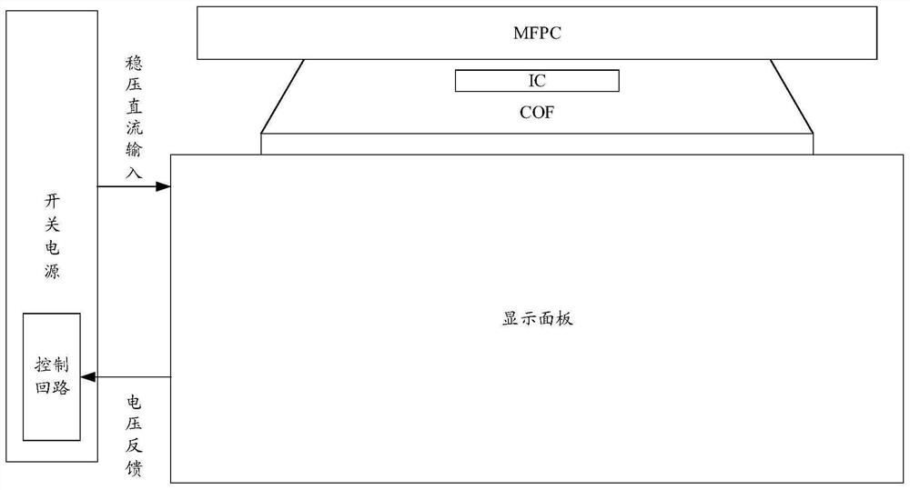
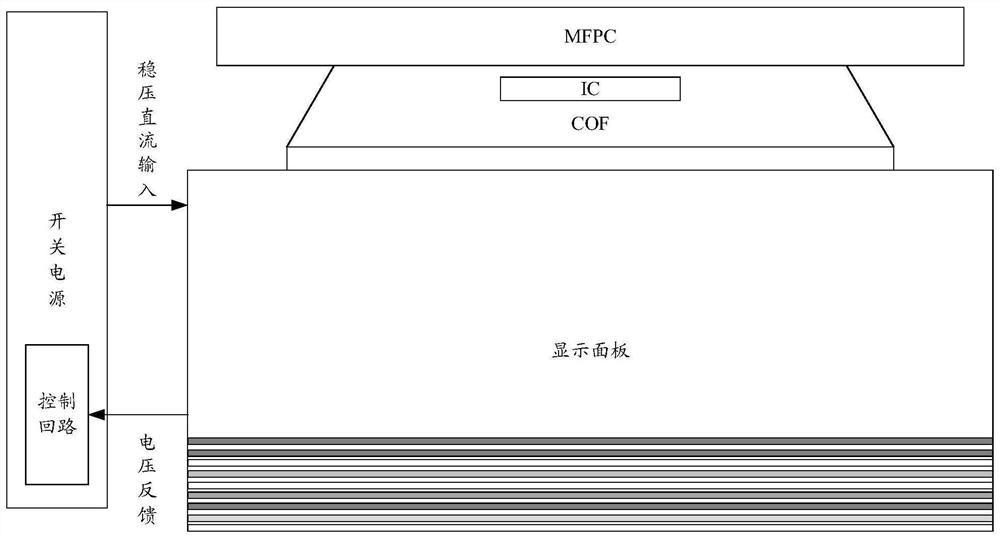
[0041] Such as figure 1 As shown, when an OLED (organic light emitting diode) display panel is applied to a display device such as a mobile phone or a tablet computer, a switching power supply provides a stable DC output voltage to realize power supply. The display device mainly includes a control circuit board. In this embodiment, it...
PUM
 Abstract
Description
Claims
Application Information
 - Generate Ideas
- Intellectual Property
- Life Sciences
- Materials
- Tech Scout
- Unparalleled Data Quality
- Higher Quality Content
- 60% Fewer Hallucinations
Browse by: Latest US Patents, China's latest patents, Technical Efficacy Thesaurus, Application Domain, Technology Topic, Popular Technical Reports.
© 2025 PatSnap. All rights reserved.Legal|Privacy policy|Modern Slavery Act Transparency Statement|Sitemap|About US| Contact US: help@patsnap.com