Image forming control method, consumable chip, image forming device and consumable
A consumable chip and image technology, which is applied in the direction of electric recording process applying charge pattern, equipment for applying charge pattern electric recording process, electric recording technique, etc. Record the life of consumables and other issues to avoid interception and tampering and secure data transmission
- Summary
- Abstract
- Description
- Claims
- Application Information
AI Technical Summary
Problems solved by technology
Method used
Image
Examples
Embodiment 1
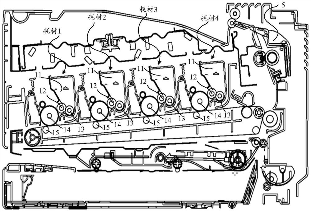
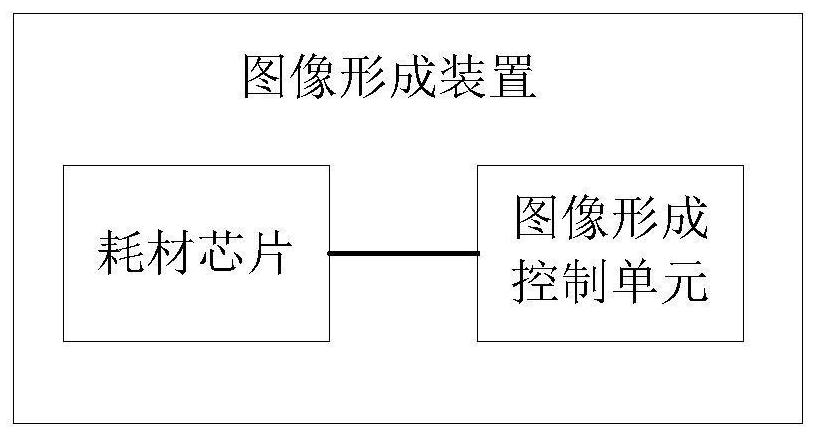
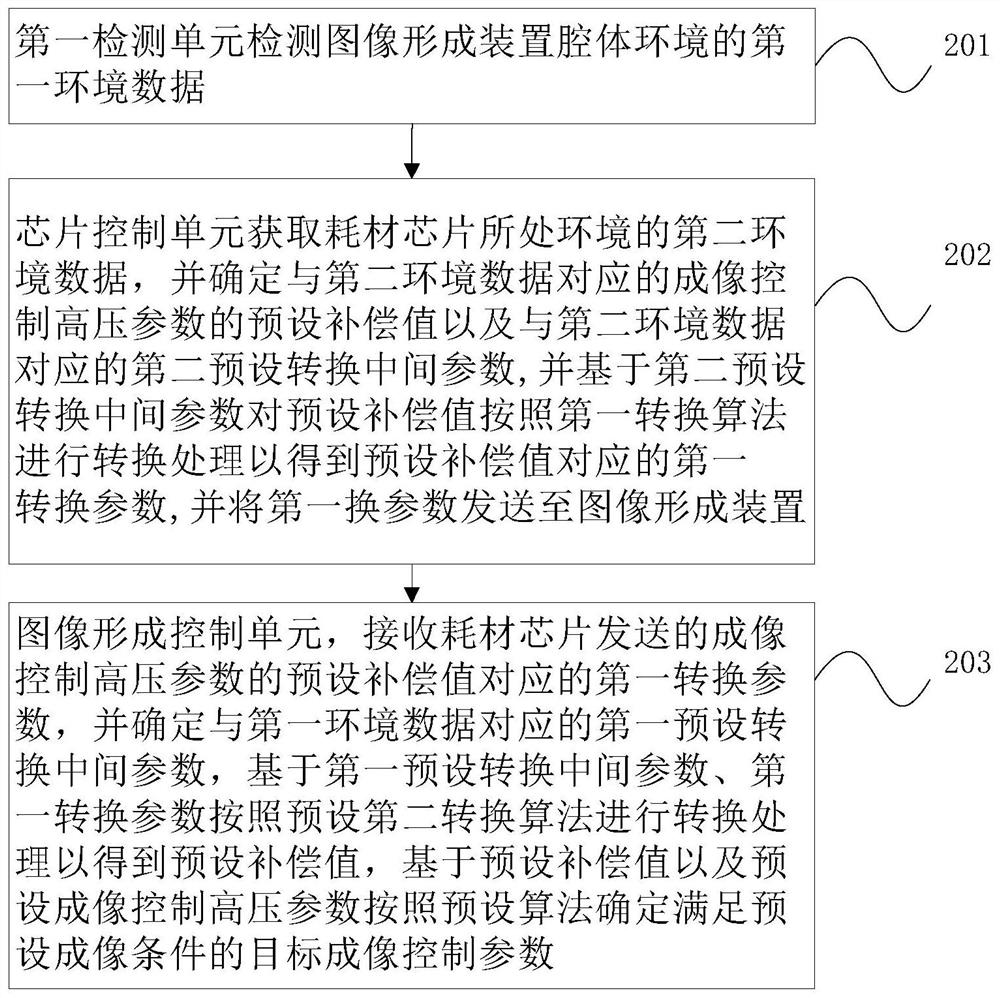
[0044] image 3 It is a schematic flow chart of an image formation control method provided in the embodiment of the present application. like image 3 As shown, the method in the embodiment of the present application is applied to an image forming device and a consumable chip. The image forming device is detachably installed with a consumable, and the consumable is mounted with a chip. The image forming device includes an image forming control unit and a first detection unit. , the chip includes a chip control unit, and the method may include:
[0045] Step 201, the first detection unit detects first environment data of the cavity environment of the image forming apparatus.
[0046] In this embodiment, the first detection unit may include a sensor for real-time detection of the first environmental data of the cavity environment of the image forming device, wherein the cavity environment refers to the environment of the internal space surrounded by the casing of the image for...
Embodiment 2
[0117] Usually, after the image forming operation is completed, the image forming device also needs to write data such as the number of printed paper pages and the consumption of toner into the consumable chip. It communicates by exchanging passwords, which is easy to intercept the data for analysis and tampering, which may cause the chip of the consumables to wrongly record the information related to the life of the consumables, lead to wrongly determine the life of the consumables, and cannot correctly prompt the user to replace the consumables. Inconvenience occurs, such as the consumables that have not reached the end of their life are mistakenly considered to be out of life, prompting the user to replace the consumables, and / or the consumables that are approaching the end of their life are mistakenly considered to be usable, and the user is not prompted to replace the consumables in time .
[0118] In order to solve the above technical problems, such as Figure 7 As show...
Embodiment 3
[0173] Figure 5 It is a schematic structural diagram of an image forming apparatus provided in an embodiment of the present application. like Figure 5 As shown, the image forming device provided in this embodiment may include: a first detection unit module 41, a second detection unit 42, and an image forming control unit 43. The image forming device is detachably installed on a consumable, and the consumable is installed with The consumable chip, the consumable chip includes a chip control unit 44 .
[0174] The first detection unit module 41 is configured to detect and obtain first environmental data of the environment in the cavity of the image forming device;
[0175] The second detection unit 42 is configured to detect the second environmental data of the environment where the consumable chip is located;
[0176]The chip control unit 44 is configured to acquire the second environment data of the environment where the consumable chip is located, and determine the prese...
PUM
 Abstract
Description
Claims
Application Information


