Photosensitive conductive structure and touch sensor

A conductive structure, photosensitive technology, applied in the direction of instrument, electrical digital data processing, data processing input/output process, etc., can solve problems such as unstable contact impedance, and achieve the effect of overcoming high contact impedance

Pending Publication Date: 2022-03-01
CAMBRIOS FILM SOLUTIONS XIAMEN CORP
View PDF0 Cites 0 Cited by
  • Summary
  • Abstract
  • Description
  • Claims
  • Application Information

AI Technical Summary

Problems solved by technology

[0003] In order to improve the problem of unstable contact impedance caused by inaccurate screen printing alignment in the peripheral circuit area of ​​the traditional photosensitive conductive structure, the present invention provides a photosensitive conductive structure and a touch sensor

Method used


Image

  • Photosensitive conductive structure and touch sensor
  • Photosensitive conductive structure and touch sensor
  • Photosensitive conductive structure and touch sensor

Examples


Embodiment 1

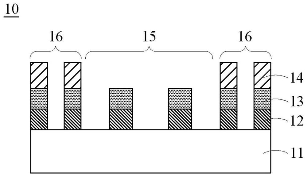
[0086] figure 1 It is a schematic diagram of the photosensitive conductive structure of Embodiment 1 of the present invention. Such as figure 1 As shown, the photosensitive conductive structure 10 of Embodiment 1 of the present invention includes: a substrate 11; a lift-off photosensitive resin layer 12, which is arranged on the substrate 11; a nano-silver layer 13, which is arranged on On the lift-off type photosensitive resin layer 12; and a photosensitive conductive layer 14, which is arranged on the edge of the nano-silver layer 13, so as to define that the nano-silver layer 13 is not covered by the photosensitive conductive structure 10 A visible area 15 covered by the photosensitive conductive layer 14 , and a peripheral circuit area 16 covered by the photosensitive conductive layer 14 of the nano-silver layer 13 . Wherein, the average molecular weight (Mn) of the lift-off photosensitive resin layer 12 is greater than 3,000 and less than 100,000. Wherein, the photosen...

Embodiment 2

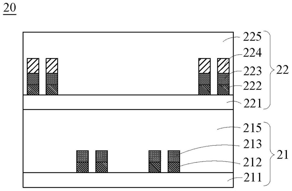
[0103] image 3 It is a schematic diagram of the touch sensor according to Embodiment 2 of the present invention. Such as image 3 As shown, the touch sensor 20 of this embodiment includes: a first photosensitive conductive structure 21 ; and a second photosensitive conductive structure 22 disposed on the first photosensitive conductive structure 21 . Wherein, the first photosensitive conductive structure 21 includes: a first substrate 211; a first lift-off photosensitive resin layer 212, which is arranged on the first substrate 211; a first nano-silver layer 213, which disposed on the first lift-off photosensitive resin layer 212 ; and a first optical adhesive 215 (Optically Clear Adhesive, OCA), disposed on the first nano-silver layer 213 . Wherein, the second photosensitive conductive structure 22 includes: a second substrate 221; a second lift-off photosensitive resin layer 222, which is arranged on the second substrate 221; a second nano silver layer 223, which Set on ...

Embodiment 3

[0108] Figure 4 It is a schematic diagram of a touch sensor according to Embodiment 3 of the present invention. Such as Figure 4 As shown, the photosensitive conductive structure 30 of this embodiment includes: a substrate 31; a first lift-off photosensitive resin layer 312, which is arranged on the substrate 31; a first nano-silver layer 313, which is arranged On the first lift-off photosensitive resin layer 312; a first photosensitive conductive layer 314, which is arranged on the edge of the first nano-silver layer 313, to define the first photosensitive conductive structure 30 A visible region 315 where a silver nanometer layer 313 is not covered by the first photosensitive conductive layer 314, and a peripheral circuit region 316 where the first nanosilver layer 313 is covered by the first photosensitive conductive layer 314; Two lift-off photosensitive resin layers 322, which are arranged under the substrate 31; a second nano-silver layer 323, which is arranged under...


PUM


Abstract

A photosensitive conductive structure includes: a substrate; the lifting type photosensitive resin layer is arranged on the base material; the nano-silver layer is arranged on the lifting type photosensitive resin layer; the photosensitive conductive layer is arranged on the edge of the nano-silver layer so as to define a visible area, not covered by the photosensitive conductive layer, of the nano-silver layer in the photosensitive conductive structure and a peripheral circuit area, covered by the photosensitive conductive layer, of the nano-silver layer in the photosensitive conductive structure, the average molecular weight (Mn) of the flip-off photosensitive resin layer is greater than 3,000 and less than 100,000, and the flip-off photosensitive resin layer, the nano-silver layer and the photosensitive conductive layer are patterned. The touch sensor comprises at least one layer of the photosensitive conductive structure.

Description

technical field [0001] The invention relates to a photosensitive conductive structure, in particular to a photosensitive conductive structure comprising a lift-off photosensitive resin layer. The present invention also relates to a touch sensor comprising the above-mentioned photosensitive conductive structure. Background technique [0002] The photosensitive conductive structure can be applied to touch sensors. The peripheral circuit area of ​​the photosensitive conductive structure in the traditional touch sensor is made by screen printing, which may cause unstable contact impedance due to inaccurate screen printing alignment, which may lead to signal loss and distortion. Contents of the invention [0003] In order to improve the problem of unstable contact impedance caused by inaccurate screen printing alignment in the peripheral circuit area of ​​the traditional photosensitive conductive structure, the present invention provides a photosensitive conductive structure a...

Claims


Application Information

Patent Timeline
Patent Type & Authority Applications(China)
IPC IPC(8): G06F3/041G06F3/042
CPCG06F3/041G06F3/042
Inventor 萧仲钦练修成蔡家扬徐淑屏
Owner CAMBRIOS FILM SOLUTIONS XIAMEN CORP
Why Eureka
Try Eureka