

Multi-chip three-dimensional packaging structure and packaging method
An encapsulation method and encapsulation structure technology, which can be applied in the manufacture of electrical solid devices, semiconductor devices, and semiconductor/solid state devices, etc., can solve the problems of excessively long conductive lines, scattered lines, and complexity, and shorten the lead length, reduce the difficulty of packaging, The effect of simplifying the packaging process
- Summary
- Abstract
- Description
- Claims
- Application Information
AI Technical Summary
Problems solved by technology
Method used
Image

Examples
Embodiment Construction
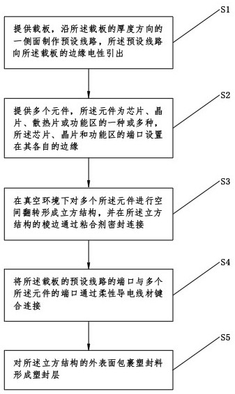
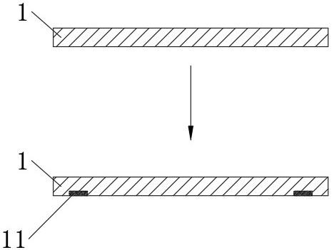
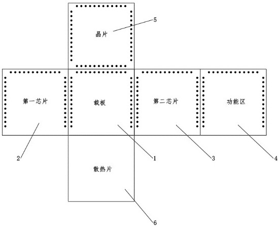
[0035] The following will clearly and completely describe the technical solutions in the embodiments of the present invention with reference to the accompanying drawings in the embodiments of the present invention. Obviously, the described embodiments are only some, not all, embodiments of the present invention. The components of the embodiments of the invention generally described and illustrated in the figures herein may be arranged and designed in a variety of different configurations. Accordingly, the following detailed description of the embodiments of the invention provided in the accompanying drawings is not intended to limit the scope of the claimed invention, but merely represents selected embodiments of the invention. Based on the embodiments of the present invention, all other embodiments obtained by those skilled in the art without making creative efforts belong to the protection scope of the present invention.
[0036] It should be noted that like numerals and let...
PUM
 Abstract
Description
Claims
Application Information