Supercharge Your Innovation With Domain-Expert AI Agents!

Method for enhancing special distribution defect detection

A defect detection and special technology, applied in the direction of semiconductor/solid-state device testing/measurement, electrical components, circuits, etc., can solve the problems of lack of pertinence and poor timeliness, and achieve enhanced sampling inspection, strong timeliness, and increased sample size. Effect

Pending Publication Date: 2022-03-04
SHANGHAI HUALI MICROELECTRONICS CORP
View PDF0 Cites 0 Cited by
  • Summary
  • Abstract
  • Description
  • Claims
  • Application Information

AI Technical Summary

Problems solved by technology

[0007] The present invention aims at providing a method for enhancing the detection of special distribution defects in the prior art, such as poor timeliness and lack of pertinence in sampling in the traditional defect monitoring process

Method used


Image

  • Method for enhancing special distribution defect detection
  • Method for enhancing special distribution defect detection
  • Method for enhancing special distribution defect detection

Examples


Embodiment Construction

[0028] In order to illustrate the technical content, structural features, achieved goals and effects of the present invention in detail, the following will be described in detail in conjunction with the embodiments and accompanying drawings.

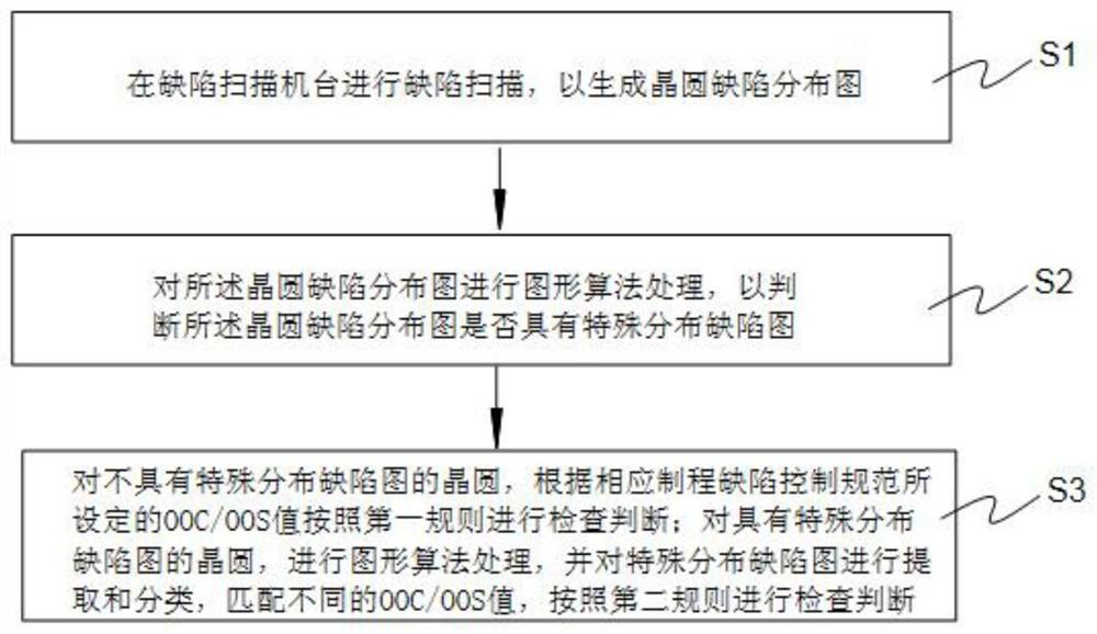
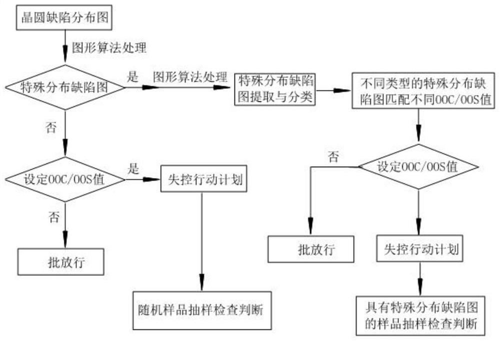
[0029] see figure 1 , figure 2 , figure 1 Shown is a flow chart of the method for enhancing the detection of special distribution defects in the present invention. figure 2 Shown is a schematic diagram of the mechanism of the method for enhancing the detection of special distributed defects in the present invention. The method for enhancing special distribution defect detection includes:

[0030] Execute step S1: perform defect scanning on the defect scanning machine to generate a wafer defect distribution map;

[0031] Executing step S2: performing graphical algorithm processing on the wafer defect distribution map to determine whether the wafer defect distribution map has a special distribution defect map;

[0032] Executing s...


PUM


Abstract

A method for enhancing special distribution defect detection comprises the following steps: performing defect scanning on a defect scanning machine to generate a wafer defect distribution diagram; performing graphic algorithm processing on the defect distribution diagram to judge whether the defect distribution diagram has a special distribution defect diagram or not; checking and judging the wafer without the special distribution defect graph according to the OOC / OOS value set according to the defect control specification of the corresponding process and a first rule; and performing graph algorithm processing on the wafer with the special distribution defect graph, extracting and classifying the special distribution defect graph, matching different OOC / OOS values, and checking and judging according to a second rule. According to the method, the definition of the special distribution defect graph is further increased, and different OOC / OOS values are matched to inspect and judge the wafer with the special distribution defect graph, so that the timeliness is high, the special distribution defect graph can be found in time, the sampling pertinence is high, the sampling inspection of the special distribution defect group is enhanced, and the sample size is increased.

Description

technical field [0001] The invention relates to the technical field of semiconductor manufacturing, in particular to a method for enhancing the detection of special distributed defects. Background technique [0002] In the semiconductor chip manufacturing process, the establishment of a reasonable and efficient defect monitoring system can realize real-time monitoring of the defect status of the wafer caused by process or machine abnormality, and timely confirm the cause of the defect. The defect monitoring system plays an important role in reducing defects and improving yield. [0003] At present, the conventional defect monitoring process is as follows. First, the defect scanning is performed on the defect scanning machine to generate a wafer defect map (DefectMap), and the out-of-control value (OOC, OutOfControl) and out-of-spec The value (OOS, Out Of Specification) determines whether an alarm is triggered. Wafers that are not triggered go directly to the next step, and ...

Claims


Application Information

Patent Timeline
Patent Type & Authority Applications(China)
IPC IPC(8): H01L21/66
CPCH01L22/12H01L22/20
Inventor 金鑫瞿燕刘飞珏
Owner SHANGHAI HUALI MICROELECTRONICS CORP
Features
  • R&D
  • Intellectual Property
  • Life Sciences
  • Materials
  • Tech Scout
  • Unparalleled Data Quality
  • Higher Quality Content
  • 60% Fewer Hallucinations
Learn More