Current loop communication circuit and air conditioner

A technology of current loop communication and communication circuit, which is applied in the field of current loop communication, can solve problems such as failure of current loop communication, and achieve the effect of resisting the interference of increased coupling capacitance and stabilizing current loop communication

Active Publication Date: 2022-04-05
GREE ELECTRIC APPLIANCES INC OF ZHUHAI
6 Cites 0 Cited by

AI-Extracted Technical Summary

Problems solved by technology

[0004] For this reason, this application provides a current loop communication circuit and an air conditioner, which helps to solve the current loop co...

Method used

At least one current loading circuit 13 is connected with the host side communication circuit 11, when the current loading circuit 13 receives the current loading signal, a loading current is formed on the current loading circuit 13, allowing the communication line S The communication current increases.
Carry out voltage clamping by first clamping diode TVS1, when current loading circuit 13 is opened, can form loading current, and can not be short-circuited, and then allow this loading current to be superimposed on communication line S, increase communication line S On the current, in the case of long-distance current loop communication, it can effectively resist the interference of the increased coupling capacitance and make the current loop communication stable.
Concretely, this power supply circuit 14 plays rectifying voltage stabilizing effect, and power supply circuit 14 is connected live l...

Abstract

The invention relates to a current loop communication circuit and an air conditioner, and belongs to the technical field of current loop communication. The communication circuit comprises a host side communication circuit and a slave side communication circuit, wherein the host side communication circuit and the slave side communication circuit are jointly connected with a zero line and a communication line; and the at least one current loading circuit is connected with the host side communication circuit, and when the current loading circuit receives a current loading signal, loading current is formed on the current loading circuit, so that communication current passing through a communication line is increased. The problem that under the condition of current loop communication, when a connecting line is too long, current loop communication fails due to the fact that coupling capacitance is increased is solved.

Application Domain

Mechanical apparatusSpace heating and ventilation safety systems +4

Technology Topic

TelecommunicationsCapacitance +2

Image

  • Current loop communication circuit and air conditioner
  • Current loop communication circuit and air conditioner

Examples

  • Experimental program(1)

Example Embodiment

[0039] In order to make the objectives, technical solutions and advantages of the present application more clear, the technical solutions of the present application will be described in detail below. Obviously, the described embodiments are only a part of the embodiments of the present application, but not all of the embodiments. Based on the examples in this application, all other implementations obtained by those of ordinary skill in the art without creative work fall within the scope of protection of this application.
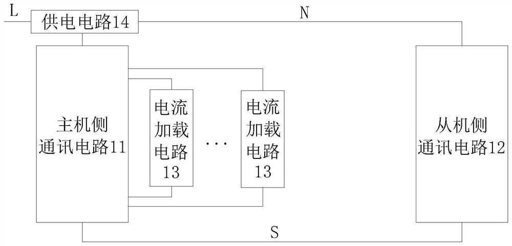
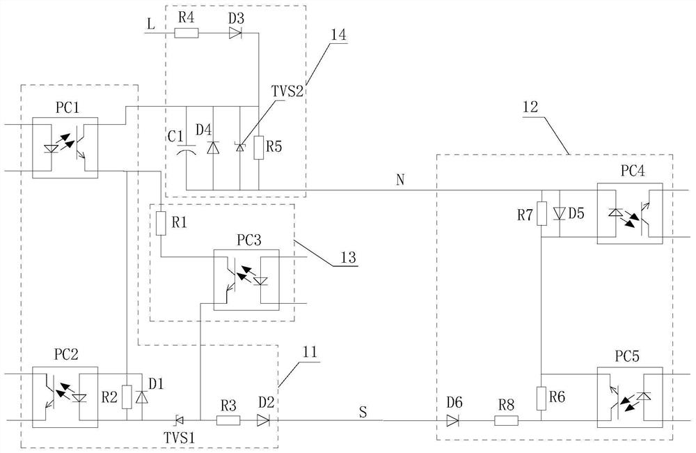
[0040] see figure 1 and figure 2 , figure 1 is a schematic diagram of the principle of a current loop communication circuit according to an exemplary embodiment, figure 2 is a specific schematic diagram of a current loop communication circuit according to an exemplary embodiment, such as figure 1 and figure 2 As shown, the current loop communication circuit includes:
[0041] The master side communication circuit 11 and the slave side communication circuit 12, the master side communication circuit 11 and the slave side communication circuit 12 are both connected to the neutral line N and the communication line S;
[0042] At least one current loading circuit 13 is connected to the communication circuit 11 on the host side. When the current loading circuit 13 receives a current loading signal, a loading current is formed on the current loading circuit 13, so that the communication current passing through the communication line S is increase.
[0043] Specifically, taking the application to an air conditioner as an example, for the master-side communication circuit 11 and the slave-side communication circuit 12 of the current loop communication circuit, when one is applied to the outdoor unit of the air conditioner, the other is applied Indoor unit for air conditioner. For example, the communication circuit 11 on the master side can be applied to the indoor unit of the air conditioner, and the communication circuit 12 on the slave side can be applied to the outdoor unit of the air conditioner. In this application, at least one current loading circuit 13 is configured for the host-side communication circuit 11, figure 2 In the shown current loop communication circuit, the current loading circuit 13 is one, and in practical applications, the current loading circuit 13 may be configured as two or more. Each time a current loop communication circuit is turned on, the communication current of the communication line S can be increased once.
[0044] In this way, whether the current loading circuit 13 is turned on can meet the application requirements of stable current loop communication under long and short communication distances. A loading current is formed on the current loading circuit 13, so as to increase the communication current through the communication line S, so as to overcome the influence of the increase of the coupling capacitance on the current loop communication when the connection line is too long. In the short case, the coupling capacitance between the lines is small, and the coupling capacitance has little interference with the current loop communication, which can prevent the current loading circuit 13 from starting. Therefore, the present application can meet the application requirements of current loop communication under long and short communication distances, and in the case of long distance current loop communication, the interference caused by the increase of coupling capacitance can be effectively resisted, and the current loop communication can be stabilized.
[0045] In order to meet the application requirements of current loop communication under long and short communication distances, in practical applications, taking the air conditioner unit as an example, after the air conditioner unit is powered on, first try to see if the master side communication circuit 11 and the slave side communication circuit 12 are The current loop communication can be established directly. If the communication can be established directly, it means that it is short-distance current loop communication. If not, it means that it is long-distance current loop communication. The communication current of the communication line S is increased. If there are multiple current loading circuits 13, the current loading circuits 13 can be turned on one by one, and each time a current loading circuit 13 is turned on, it is confirmed whether the current loop communication can be established. The circuit 13 is loaded until the establishment of current loop communication is confirmed.
[0046] The master side communication circuit 11 , the slave side communication circuit 12 and the current loading circuit 13 will be described in detail below.
[0047] Please refer to figure 2 , in one embodiment, the host-side communication circuit 11 includes:
[0048] The first optocoupler PC1, the second optocoupler PC2 and the first clamp diode TVS1, the on-off side of the first optocoupler PC1, the signal side of the second optocoupler PC2 and the first clamp The diodes TVS1 are connected in sequence, the first optocoupler PC1 is used as a signal transmitting end of the host side communication circuit 11 , and the second optocoupler PC2 is a signal receiving end of the host side communication circuit 11 .
[0049] For specifics, please refer to figure 2 , the first optocoupler PC1 is used as the signal sending end of the host-side communication circuit 11. When the on-off side of the first optocoupler PC1 is turned on, the current enters from the input end of the on-off side of the first optocoupler PC1, and passes through the first optocoupler PC1. After the signal of the second optocoupler PC2 is measured and the first clamping diode TVS1, it enters the slave side communication circuit 12 through the communication line S, and the current enters the neutral line N after passing through the slave side communication circuit 12, thereby forming a current loop communication loop .
[0050] When the master-side communication circuit 11 and the slave-side communication circuit 12 can establish a current loop communication connection, if the master-side communication circuit 11 needs to send a signal to the slave-side communication circuit 12, the signal side of the first optocoupler PC1 is controlled. In this way, the on-off control of the on-off side of the first optocoupler PC1 is realized, and the slave-side communication circuit 12 responds to the on-off of the on-off side of the first optocoupler PC1 to obtain a corresponding communication signal.
[0051] The second optocoupler PC2 is used as the signal receiving end of the host-side communication circuit 11. If the host-side communication circuit 11 needs to receive a signal from the slave-side communication circuit 12, the on-off side of the first optocoupler PC1 is kept on. In this way, Only the second optocoupler PC2 can respond to the signal sending action of the slave-side communication circuit 12 to obtain a corresponding communication signal.
[0052] The voltage is clamped by the first clamping diode TVS1. When the current loading circuit 13 is turned on, a loading current can be formed without being short-circuited, so that the loading current is superimposed on the communication line S, and the current on the communication line S is increased. In the case of long-distance current loop communication, it can effectively resist the interference of the increased coupling capacitance, so that the current loop communication is stable.
[0053] Please refer to figure 2 In one embodiment, the current loading circuit 13 is connected in parallel with the series circuit formed by the signal side of the second optocoupler PC2 and the first clamping diode TVS1.
[0054] In this embodiment, the current loading circuit 13 is controlled by the first optocoupler PC1. In the case of long-distance current loop communication, a current loading signal is applied to the current loading circuit 13 to keep it normally turned on. When the on-off side of the PC1 is turned on, a loading current is formed on the current loading circuit 13 , and the loading current is superimposed on the communication line S to increase the current on the communication line S.
[0055] see figure 2 , in one embodiment, the current loading circuit 13 includes:
[0056] A third optocoupler PC3 and a first resistor R1, the on-off side of the third optocoupler PC3 is connected in series with the first resistor R1, and the signal side of the third optocoupler PC3 is used for receiving the current loading When the signal is received, the on-off side of the third optocoupler PC3 is controlled to be turned on.
[0057] Specifically, in the case of long-distance current loop communication, a current loading signal is applied to the current loading circuit 13 to keep it normally turned on.
[0058] see figure 2 , in one embodiment, the host-side communication circuit 11 further includes:
[0059] The second resistor R2 is connected in parallel with the signal side of the second optocoupler PC2;
[0060] The cathode of the first diode D1 is connected to the signal-side input terminal of the second optocoupler PC2, and the anode is connected to the signal-side output terminal of the second optocoupler PC2.
[0061] Specifically, the second resistor R2 and the first diode D1 can discharge the current, provide a discharge path for the weak current, and prevent the second optocoupler PC2 from being misconnected.
[0062] see figure 2 , in one embodiment, the host-side communication circuit 11 further includes:
[0063] The third resistor R3 and the second diode D2 form a series circuit and are connected to the first clamping diode TVS1.
[0064] Specifically, the third resistor R3 forms a current limiting protection effect on the communication line S, and the second diode D2 constrains the direction of the current to flow from the host-side communication circuit 11 to the slave-side communication circuit 12 .
[0065] see figure 2 , in one embodiment, the current loop communication circuit further comprises:
[0066] The power supply circuit 14 includes:
[0067] a fourth resistor R4, a third diode D3, a fifth resistor R5, a second clamping diode TVS2, a fourth diode D4 and a first capacitor C1;
[0068] Wherein, one end of the fourth resistor R4 is used to connect to the live wire L, and the other end is connected to the anode of the third diode D3;
[0069] The fifth resistor R5, the second clamping diode TVS2, the fourth diode D4 and the first capacitor C1 are connected in parallel to form a parallel circuit, one end of the parallel circuit is connected to the negative electrode of the third diode D3 And the communication current input end of the host side communication circuit 11 is connected in common, and the other end of the parallel connection circuit is connected with the neutral line N.
[0070] Specifically, the power supply circuit 14 plays the role of rectifying and stabilizing, the power supply circuit 14 is connected to the live wire L, the fourth resistor R4 forms current limiting protection for the third diode D3, the third diode D3 rectifies the alternating current, and the third diode D3 rectifies the alternating current. The two clamping diodes TVS2 form the clamping voltage, the first capacitor C1 performs filtering, the fifth resistor R5 and the fourth diode D4 play a protective role, filter out interference, and at the same time, transmit the current signal from the neutral line N to the host side communication circuit 11 .
[0071] see figure 2 , in one embodiment, the slave-side communication circuit 12 includes:
[0072] The fourth optocoupler PC4, the fifth optocoupler PC5, and the sixth resistor R6, wherein the signal side of the fourth optocoupler PC4 is connected to the on-off side of the fifth optocoupler PC5, and the sixth resistor R6 is connected to the on-off side of the fifth optocoupler PC5. The on-off sides of the fifth optocoupler PC5 are connected in parallel, the fourth optocoupler PC4 is used as the signal receiving end of the slave side communication circuit 12, and the fifth optocoupler PC5 is used as the slave side communication circuit 12 signal transmitter.
[0073] Specifically, during the period when the host-side communication circuit 11 sends a signal to the slave-side communication circuit 12, the on-off side of the fifth optocoupler PC5 in the slave-side communication circuit 12 is controlled to be turned on, so as to short-circuit the sixth resistor R6, so that the A relatively large current is formed on the communication line S until the host-side communication circuit 11 has sent all the data.
[0074] When a high-level signal appears on the signal side of the first optocoupler PC1 of the host-side communication circuit 11, the on-off side of the first optocoupler PC1 is turned on, and the fifth optocoupler PC5 of the slave-side communication circuit 12 is turned on. The current communication loop is activated, and the current flows through the signal side of the fourth optocoupler PC4 of the communication circuit 12 on the slave side, so that the on-off side of the fourth optocoupler PC4 is turned on, and the high voltage sent by the communication circuit 11 on the host side is received. flat signal.
[0075] When a low-level signal appears on the signal side of the first optocoupler PC1 of the host-side communication circuit 11, the on-off side of the first optocoupler PC1 is disconnected, the current communication loop is disconnected, and the fourth opto-coupler PC1 of the slave-side communication circuit 12 is disconnected. The on-off side of the optocoupler PC4 is disconnected to form a low-level signal sent by the host-side communication circuit 11 .
[0076] During the period when the slave-side communication circuit 12 sends a signal to the host-side communication circuit 11 , the on-off side of the first optocoupler PC1 in the host-side communication circuit 11 is controlled to continue to conduct until the slave-side communication circuit 12 sends all data.
[0077] When a high-level signal appears on the signal side of the fifth optocoupler PC5 of the communication circuit 12 on the slave side, the on-off side of the fifth optocoupler PC5 is turned on, the current communication loop is activated, and the current flows through the communication circuit 11 on the host side. On the signal side of the second optocoupler PC2, the on-off side of the second optocoupler PC2 is turned on, so as to receive a high-level signal sent by the communication circuit 12 on the slave side.
[0078] When a low-level signal appears on the signal side of the fifth optocoupler PC5 of the slave-side communication circuit 12, the on-off side of the fifth optocoupler PC5 is disconnected, the sixth resistor R6 intervenes, and the communication current in the current communication loop is small, A small current flows through the signal side of the second optocoupler PC2 of the host-side communication circuit 11, so that the on-off side of the second optocoupler PC2 cannot be turned on, that is, the on-off side of the second optocoupler PC2 is off. In the open state, a low-level signal sent by the communication circuit 12 on the slave side is received.
[0079] see figure 2 , in one embodiment, the slave-side communication circuit 12 further includes:
[0080] The seventh resistor R7 is connected in parallel with the signal side of the fourth optocoupler PC4;
[0081] In the fifth diode D5, the negative electrode is connected to the signal side input end of the fourth optocoupler PC4, and the positive electrode is connected to the signal side output end of the fourth optocoupler PC4.
[0082] Specifically, the seventh resistor R7 and the fifth diode D5 can discharge the current, provide a discharge path for the weak current, and prevent the fourth optocoupler PC4 from being misconnected.
[0083] see figure 2 , in one embodiment, the host-side communication circuit 11 further includes:
[0084] The eighth resistor R8 and the sixth diode D6 form a series circuit and are connected to the on-off side of the fifth optocoupler PC5.
[0085] Specifically, the eighth resistor R8 forms a current limiting protection effect on the communication line S, and the sixth diode D6 constrains the direction of the current to flow from the host-side communication circuit 11 to the slave-side communication circuit 12 .
[0086] In addition, the present application also discloses an air conditioner, comprising: the current loop communication circuit according to any one of the above, wherein, for the current loop communication circuit, the master-side communication circuit 11 and the slave-side communication circuit 12. When one is applied to the outdoor unit of the air conditioner, the other is applied to the indoor unit of the air conditioner.
[0087] Specifically, for example, the communication circuit 11 on the master side can be applied to the indoor unit of the air conditioner, and the communication circuit 12 on the slave side can be applied to the outdoor unit of the air conditioner, and the power supply source is obtained from the indoor unit of the air conditioner.
[0088] For the air conditioner of the present application, the application of the long- and short-distance current loop communication has been described in the above-mentioned relevant embodiments, and will not be repeated here.
[0089] It can be understood that, the same or similar parts in the above embodiments may refer to each other, and the content not described in detail in some embodiments may refer to the same or similar content in other embodiments.
[0090] It should be noted that, in the description of the present application, the terms "first", "second" and the like are only used for the purpose of description, and should not be construed as indicating or implying relative importance. In addition, in the description of the present application, unless otherwise specified, the meanings of "plurality" and "multiple" refer to at least two.
[0091] It will be understood that when an element is referred to as being "fixed to" or "disposed to" another element, it can be directly on the other element or intervening elements may also be present; when an element is referred to as being "connected" to another element, it will be This may be directly connected to another element or intervening elements may also be present, in addition, "connected" as used herein may include wireless connections; use of the word "and/or" includes any of one or more of the associated listed items. One unit and all combinations.
[0092] Any description of a process or method in the flowcharts or otherwise described herein may be understood to represent a module, segment or portion of code comprising one or more executable instructions for implementing a particular logical function or step of the process , and the scope of the preferred embodiments of the present application includes alternative implementations in which the functions may be performed out of the order shown or discussed, including performing the functions substantially concurrently or in the reverse order depending upon the functions involved, which should It is understood by those skilled in the art to which the embodiments of the present application belong.
[0093] It should be understood that various parts of this application may be implemented in hardware, software, firmware, or a combination thereof. In the above-described embodiments, various steps or methods may be implemented in software or firmware stored in memory and executed by a suitable instruction execution system. For example, if implemented in hardware, as in another embodiment, it can be implemented by any one or a combination of the following techniques known in the art: Discrete logic circuits, application specific integrated circuits with suitable combinational logic gates, Programmable Gate Arrays (PGA), Field Programmable Gate Arrays (FPGA), etc.
[0094] Those of ordinary skill in the art can understand that all or part of the steps carried by the methods of the above embodiments can be completed by instructing the relevant hardware through a program, and the program can be stored in a computer-readable storage medium, and the program is stored in a computer-readable storage medium. When executed, one or a combination of the steps of the method embodiment is included.
[0095] In addition, each functional unit in each embodiment of the present application may be integrated into one processing module, or each unit may exist physically alone, or two or more units may be integrated into one module. The above-mentioned integrated modules can be implemented in the form of hardware, and can also be implemented in the form of software function modules. If the integrated modules are implemented in the form of software functional modules and sold or used as independent products, they may also be stored in a computer-readable storage medium.
[0096] The above-mentioned storage medium may be a read-only memory, a magnetic disk or an optical disk, and the like.
[0097] In the description of this specification, description with reference to the terms "one embodiment," "some embodiments," "example," "specific example," or "some examples", etc., mean specific features described in connection with the embodiment or example , structure, material or feature is included in at least one embodiment or example of the present application. In this specification, schematic representations of the above terms do not necessarily refer to the same embodiment or example. Furthermore, the particular features, structures, materials or characteristics described may be combined in any suitable manner in any one or more embodiments or examples.
[0098] Although the embodiments of the present application have been shown and described above, it should be understood that the above embodiments are exemplary and should not be construed as limitations to the present application. Embodiments are subject to variations, modifications, substitutions and variations.

PUM

no PUM

Description & Claims & Application Information

We can also present the details of the Description, Claims and Application information to help users get a comprehensive understanding of the technical details of the patent, such as background art, summary of invention, brief description of drawings, description of embodiments, and other original content. On the other hand, users can also determine the specific scope of protection of the technology through the list of claims; as well as understand the changes in the life cycle of the technology with the presentation of the patent timeline. Login to view more.
Why Eureka
Try Eureka