Design method of photonic crystal structure with topological interface state
A photonic crystal and structure design technology, applied in optics, optical components, instruments, etc., can solve the problem of unrealized manipulation of topological interface states, and achieve the effect of adjustability
- Summary
- Abstract
- Description
- Claims
- Application Information
AI Technical Summary
Problems solved by technology
Method used
Image

Examples
Embodiment 1
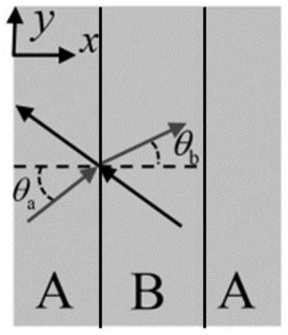
[0038] like figure 1 As shown, a method for designing a photonic crystal structure with topological interface states includes the following steps:
[0039] S1: Build a one-dimensional PC unit with two different dielectric layers;
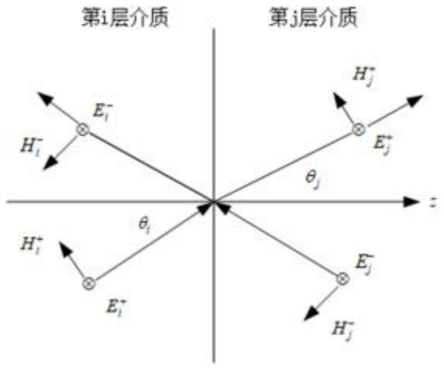
[0040] It should be noted that it is preferred to use two different dielectric layers to construct a one-dimensional PC unit, such as figure 1 The shown (A represents the first dielectric layer, B represents the second dielectric layer) is a one-dimensional PC unit in TE mode, wherein the two different media have different refractive indices, when the electric field wave vector is at the included angle θ i through a section of thickness d i , the refractive index is n i When the medium is , the one-dimensional PC unit phase change transmission matrix is:
[0041]
[0042] The phase-change transfer matrix of the complex periodic structure of the one-dimensional topological interface state is obtained by multiplying the transfer matrix of eac...
Embodiment 2
[0050] In this embodiment, the first dielectric layer is silicon dioxide, and its refractive index is n a =1.46, the second dielectric layer is titanium dioxide, the refractive index n b =2.4, if there is an interface state in the energy band diagram of the arrangement of the first dielectric layer and the second dielectric layer at the set angle, the following predicted intersection formula should be satisfied:
[0051]
[0052] where m 1 respectively represent the mth required for the existence of an interface state in the energy band diagram of the PC unit composed of the first dielectric layer and the second dielectric layer at a set angle 1 energy band, m 2 Represents the mth required for the existence of an interface state in the energy band diagram of the PC unit composed of the first dielectric layer and the second dielectric layer at a set angle 2 Strip energy band, α represents the band number scale factor.
[0053] In a specific experiment, in order to obtain...
Embodiment 3
[0060] In this embodiment, on the basis of the above-mentioned embodiment, the topological interface state of the composite periodic structure is analyzed through experiments in TE and TM modes.
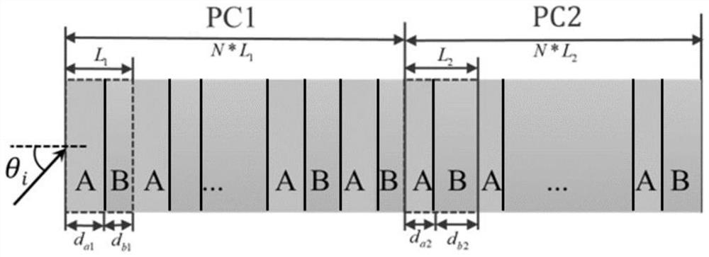
[0061] like Figure 4 As shown in (a) and (b), PC1 (that is, the combination of N first PC units) in the TE and TM modes is a partial enlarged view of the relationship between the energy band and the incident angle. There is a closed point in TE, while in the same case TM Open. Therefore, the TE has an "open-closed-open" state, while the TM mode at this angular frequency is always in the "closed" state.
[0062] If the band gap of TM is always open but not closed, there must be no interface state, and TE may have interface state. Whether the specific topological phase changes needs further analysis and research. like Figure 5 In the middle (a) is the schematic diagram of the energy band of PC1 in TE mode, the circled part is the partially enlarged part, Figure 5 In (c) a partia...
PUM
 Abstract
Description
Claims
Application Information
 - R&D
- Intellectual Property
- Life Sciences
- Materials
- Tech Scout
- Unparalleled Data Quality
- Higher Quality Content
- 60% Fewer Hallucinations
Browse by: Latest US Patents, China's latest patents, Technical Efficacy Thesaurus, Application Domain, Technology Topic, Popular Technical Reports.
© 2025 PatSnap. All rights reserved.Legal|Privacy policy|Modern Slavery Act Transparency Statement|Sitemap|About US| Contact US: help@patsnap.com