Chip security test circuit and logic chip

A security testing and chip technology, applied in the direction of electronic circuit testing, etc., can solve the problems of complex design, decreased test coverage, and increased scan test cost.

Pending Publication Date: 2022-07-29
上海先楫半导体科技有限公司
View PDF0 Cites 2 Cited by
  • Summary
  • Abstract
  • Description
  • Claims
  • Application Information

AI Technical Summary

Problems solved by technology

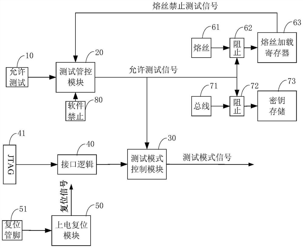
[0005] In view of the above-mentioned shortcomings of the prior art, the purpose of the present invention is to provide a chip security test circuit and a logic chip, which is used to solve the problem of decreased test coverage or complex design during the digital logic chip security test in the prior art, scan test The mode entry process takes a long time and increases the technical problem of scanning test cost

Method used


Image

  • Chip security test circuit and logic chip
  • Chip security test circuit and logic chip
  • Chip security test circuit and logic chip

Examples


Embodiment Construction

[0031] The embodiments of the present invention are described below through specific specific examples, and those skilled in the art can easily understand other advantages and effects of the present invention from the contents disclosed in this specification. The present invention can also be implemented or applied through other different specific embodiments, and various details in this specification can also be modified or changed based on different viewpoints and applications without departing from the spirit of the present invention.

[0032] see Figure 1-4 . It should be noted that the drawings provided in this embodiment are only to illustrate the basic concept of the present invention in a schematic way, so the drawings only show the components related to the present invention rather than the number, shape and the number of components in actual implementation. For dimension drawing, the type, quantity and proportion of each component can be changed at will in actual i...


PUM


Abstract

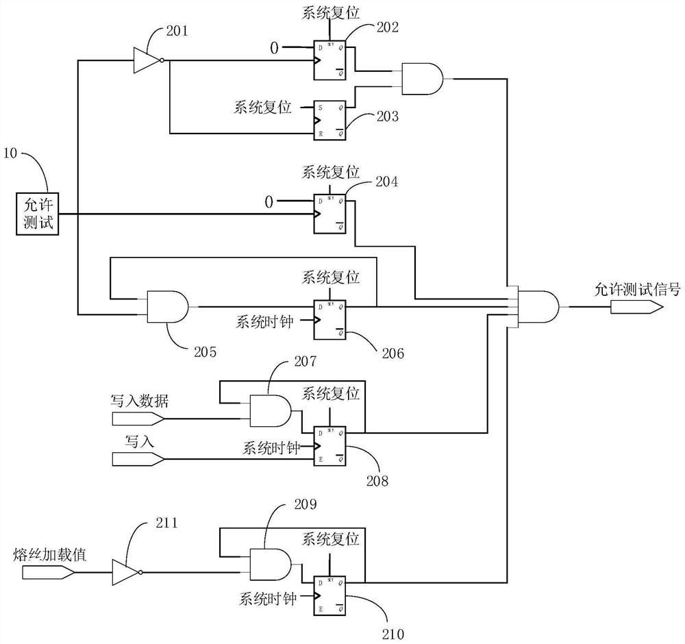
The invention discloses a chip security test circuit and a logic chip. The chip security test circuit comprises a test-allowed pin arranged on a chip; the test management and control module is configured to control the output state of the output allowed test signal according to the input signal of the allowed test pin, and convert the output allowed test signal into an effective state only when the chip is subjected to global reset; and the test mode control module is configured to control the chip to enter a test mode according to an input signal of a test mode interface of the chip when the test allowing signal output by the test management and control module is in an effective state, and control the chip to exit the test mode only when the chip is subjected to global reset. According to the invention, the test-allowed pin is arranged, and the test mode and the normal working mode are selected during power-on reset every time, so that sensitive data are prevented from being transmitted between the test mode and the normal working mode, and the purpose of information security is achieved.

Description

technical field [0001] The invention relates to the technical field of chip security testing, in particular to a chip security testing circuit and a logic chip. Background technique [0002] In addition to the functional mode (normal working mode) during normal operation, the digital logic chip usually also has a test mode for screening defective products or analyzing product failures in the production stage. In this mode, the registers and logic units inside the chip will work in another way, so that the registers inside the chip can observe the state or exert control through the chip pins to the maximum extent. [0003] For the registers used to store sensitive information (such as keys, etc.) in the working mode, if the test mode is used unreasonably, it may become an attack method, thereby threatening information security. For example, in the normal working mode, if the sensitive information has been loaded into the register, if the chip enters the test mode at this tim...

Claims


Application Information

Patent Timeline
IPC IPC(8): G01R31/28
CPCG01R31/2851G01R31/2884G01R31/2886
Inventor 鲍立朱永峰
Owner 上海先楫半导体科技有限公司
Why Eureka
Try Eureka