Supercharge Your Innovation With Domain-Expert AI Agents!

Storage circuit with odd-even check unit array

一种单元阵列、奇偶校验的技术,应用在半导体存储器领域,能够解决无法测试、测试图形无法直接提供数据总线等问题,达到缩短测试时间的效果

Inactive Publication Date: 2006-05-10
SOCIONEXT INC
View PDF0 Cites 2 Cited by
  • Summary
  • Abstract
  • Description
  • Claims
  • Application Information

AI Technical Summary

Problems solved by technology

[0007] However, with the above-mentioned DRAM, when reading the data of the actual cell array, the data of the actual cell array may sometimes be partially corrected by a parity bit read from the parity cell array
Therefore, there is a problem: it cannot be properly tested for operation before shipment
For this reason, using the traditional self-test technology, the test pattern generated by the test circuit cannot be directly provided to the data bus connected to the parity check cell array PCA
Therefore, it is not possible to test DRAM with parity cell array PCA by internal self-test

Method used


Image

  • Storage circuit with odd-even check unit array
  • Storage circuit with odd-even check unit array
  • Storage circuit with odd-even check unit array

Examples


no. 1 example

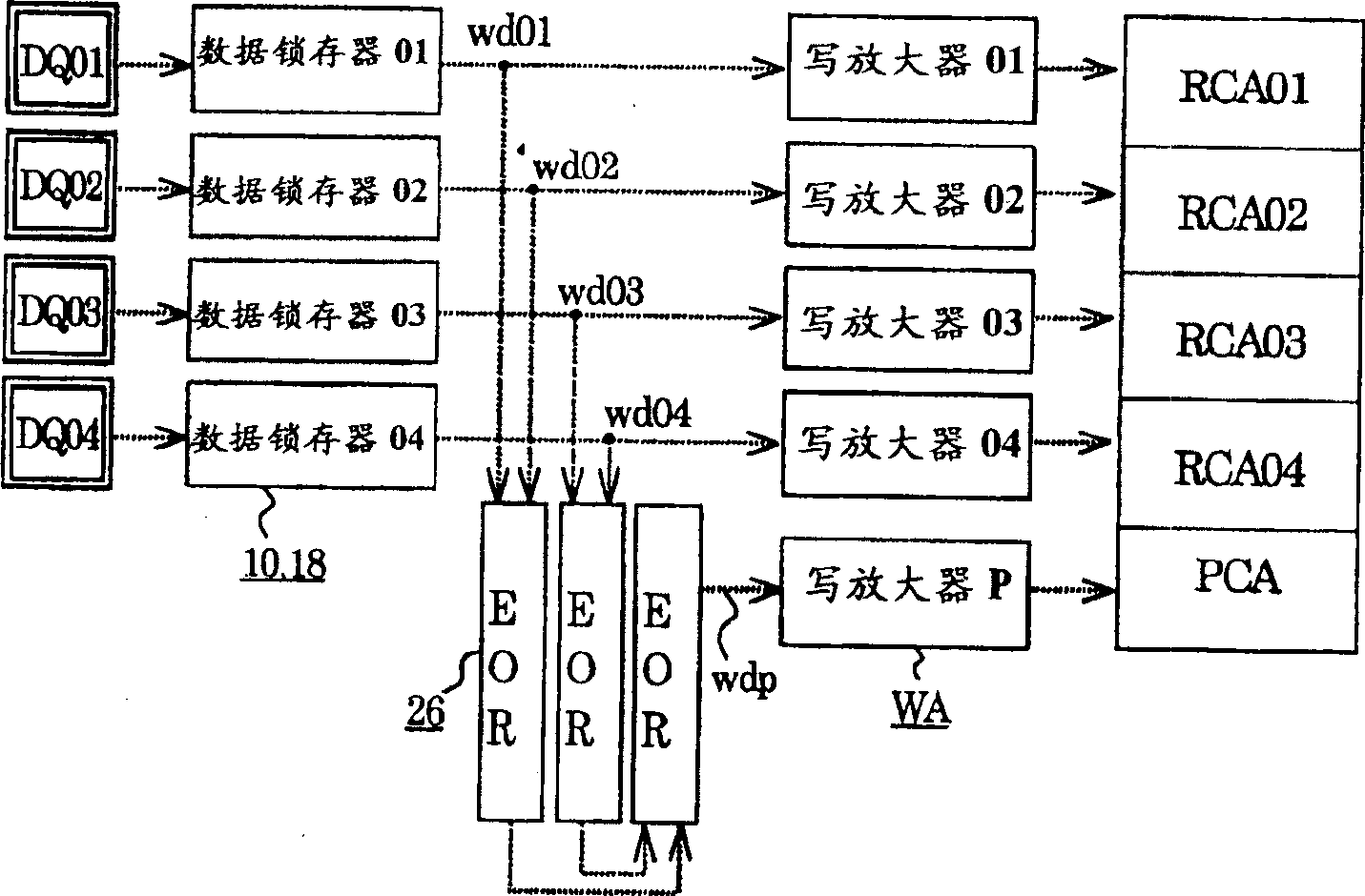
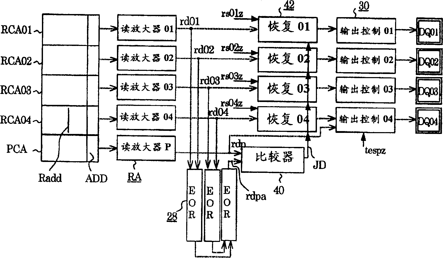
[0063] figure 1 The overall configuration of the memory circuit of the first embodiment is explained. This memory circuit has a general real cell array RCA for storing data, and has a parity cell array PCA for storing parity bits of data written in the real cell array. The cell arrays each include (not shown) a plurality of word lines, a plurality of bit lines, and 1 transistor / 1 capacitor unit located at intersections between these word lines and bit lines.

[0064] The parity bits stored in the parity cell array PCA are codes generated by computing data written into the actual cell array, ie, codes that allow error recovery in data subsequently read from the actual cell array. Therefore, in this sense, the parity cell array may be referred to as an ECC cell array storing an error correction code (ECC). That is, by storing ECC generated by more complicated logic than parity bits, even if there is a partial error in data read out from the actual cell array, the error can be ...

no. 2 example

[0101] Next, a second embodiment will be described. In the figure, signal lines indicated by thick lines are configured in various forms. In addition, some blocks connected by bold lines are composed of multiple circuits. The same reference symbols as the terminal names are used for the signals supplied via the external terminals, and the same reference symbols as the signal names are used for the signal lines that transmit the signals.

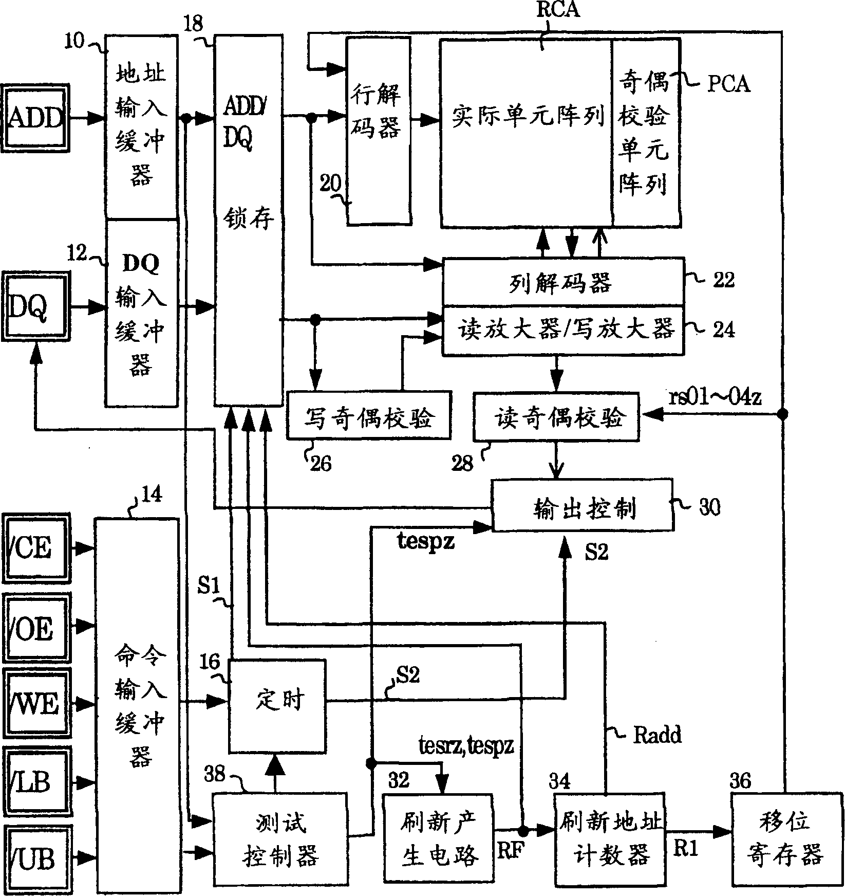
[0102] Figure 11 A second embodiment of the semiconductor memory of the present invention will be described. This semiconductor memory is formed as a DRAM on a silicon substrate using a CMOS process. The DRAM has a function of performing memory cell refresh operations without external recognition. Here, the refresh operation is an operation of rewriting data held in memory cells.

[0103] In addition, the specifications of the external terminals of the DRAM and the specifications of the signal input / output timing are made so as to confo...


PUM


Abstract

A storage circuit has: an actual cell array; a parity generation circuit for generating parity bits from data in the actual cell array; a parity cell array; a refresh control circuit for sequentially refreshing the actual cell array, and when the internal When a refresh request and a read request occur simultaneously, priority is given to a refresh operation; a data restoration part restores data read from an actual cell array according to a parity bit read from a parity cell array; and an output circuit for Output the data from the actual cell array. In addition, the memory circuit has a test control circuit that prohibits the refresh operation of the actual cell array in the first test mode to output data read from the actual cell array, and controls the output circuit in the second test mode to output data from the parity register. Test the data read out from the cell array.

Description

technical field [0001] The present invention relates to a memory circuit having a parity cell array, and more particularly, to a memory circuit capable of testing the actual cell array and the parity cell array. [0002] The present invention also relates to a semiconductor memory having a memory cell array for storing parity data of write data and having an internal self-test (BIST) function. Background technique [0003] A one-transistor type of dynamic RAM (DRAM), which is a low-cost, high-capacity memory, is widely used, but requires a refresh operation even in a power-on state due to its volatility. On the other hand, in the case of static RAM (SRAM), although the increase in capacity requires a higher cost, in the powered state, this kind of SRAM can continuously maintain the stored data, that is, it does not need to be used like DRAM. Controls the refresh operation. [0004] Conventionally, SRAM that does not require refresh control has been used in mobile phones, m...

Claims


Application Information

Patent Timeline
Patent Type & Authority Patents(China)
IPC IPC(8): G11C11/407H01L27/10G06F11/10G11C11/406G11C29/42
CPCG06F11/106G11C11/401G11C11/406G11C11/40603G11C11/40615G11C29/42G11C2211/4062
Inventor 藤冈伸也藤枝和一郎原浩太古贺彻森胜宏
Owner SOCIONEXT INC
Features
  • R&D
  • Intellectual Property
  • Life Sciences
  • Materials
  • Tech Scout
  • Unparalleled Data Quality
  • Higher Quality Content
  • 60% Fewer Hallucinations
Learn More