Magnetic storage device
A technology of magnetic storage and memory cells, which is applied in the field of semiconductor storage devices and can solve problems such as the change of data resistance becomes smaller
- Summary
- Abstract
- Description
- Claims
- Application Information
AI Technical Summary
Problems solved by technology
Method used
Image
Examples
Embodiment approach 1
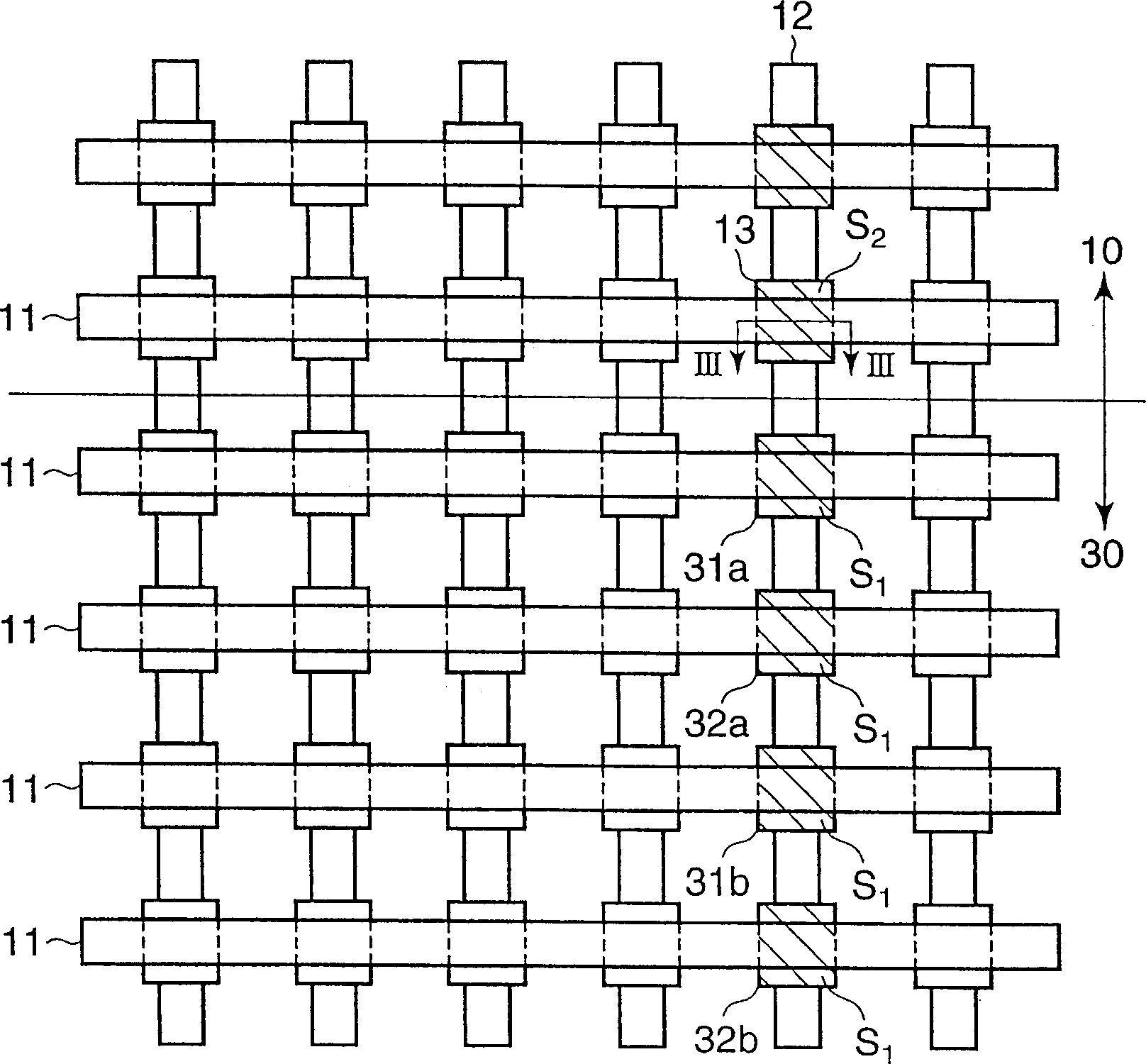
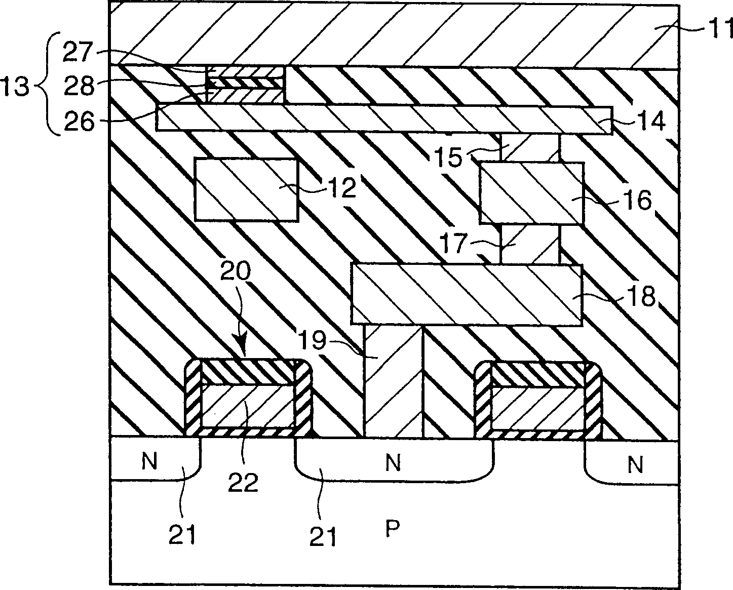
[0031] Embodiment 1 is an example in which a 1-bit (bit) memory cell portion is composed of one TMR element + 1 MOS transistor, and the reference cell portion is composed of (1 TMR element + 1 MOS transistor)×4. In addition, the so-called reference cell part refers to a cell that is selected at the same time as a 1-bit memory cell and compared with the memory cell when data is read.
[0032] figure 1 This is a circuit diagram showing the magnetic storage device according to the first embodiment of the present invention. Such as figure 1 As shown, in the magnetic storage device of the first embodiment, each 1-bit memory cell portion 10 has a TMR element 13 and a MOS transistor 20. The reference cell section 30 that determines the information written in the TMR element 13 of this memory cell section 10 has four pairs of TMR elements and MOS transistors. That is, the structure of the reference cell portion 30 includes a first pair consisting of a first TMR element 31a and MOS tran...
Embodiment approach 2
[0066] The second embodiment is an example in which a 1-bit memory cell is composed of one TMR element + 1 diode, and the reference cell part is composed of (1 TMR element + 1 diode)×4. In this second embodiment, the description of the same configuration as that of the first embodiment described above is omitted, and only the different configuration will be described.
[0067] Figure 7 This is a circuit diagram showing a magnetic storage device according to Embodiment 2 of the present invention. Such as Figure 7 As shown, in the magnetic storage device of the second embodiment, each 1-bit memory cell portion 10 has a TMR element 13 and a diode 41. The reference cell section 30 that determines the information written in the TMR element 13 of this memory cell section 10 has four sets of TMR element and diode pairs. In other words, the structure of the reference cell portion 30 includes a first pair consisting of a first TMR element 31a and a diode 42a that holds "0" data, and a s...
Embodiment approach 3
[0075] The third embodiment is an example of a configuration in which the diode is not used in the second embodiment. In this third embodiment, descriptions of the same configurations as those of the first and second embodiments described above are omitted, and only the different configurations will be described.
[0076] Picture 9 This is a circuit diagram showing a magnetic storage device according to Embodiment 3 of the present invention. Such as Picture 9 As shown, in the magnetic storage device of the third embodiment, each one-bit memory cell portion 10 has only the TMR element 13. The reference cell section 30 that determines the information written in the TMR element 13 of this memory cell section 10 has four sets of TMR elements. That is, the reference cell section 30 includes: a first TMR element 31a that holds "0" data, a second TMR element 32a that holds "1" data, a third TMR element 31b that holds "0" data, and a fourth TMR that holds "1" data. Element 32b.
[0077...
PUM
 Abstract
Description
Claims
Application Information


