Resistance change element and manufacturing method therefor

A technology of variable resistance element and manufacturing method, which is applied in the direction of electric components, electric solid-state devices, circuits, etc., and can solve the problems that the operation characteristics impair the operation stability and reliability of semiconductor storage devices, and hinder the miniaturization and large-capacity of storage devices, etc. , to achieve the effect of miniaturization

Active Publication Date: 2014-03-19
III HLDG 12 LLC
View PDF6 Cites 6 Cited by
  • Summary
  • Abstract
  • Description
  • Claims
  • Application Information

AI Technical Summary

Problems solved by technology

Such variation in operating characteristics impairs the operating stability and reliability of a semiconductor memory device constructed using a variable resistance element.
In addition, since it is necessary to add a margin as a countermeasure against such variations to the design dimensions of the variable resistance element, miniaturization and increase in capacity of memory devices are hindered.

Method used


Image

  • Resistance change element and manufacturing method therefor
  • Resistance change element and manufacturing method therefor
  • Resistance change element and manufacturing method therefor

Examples


Embodiment approach 1

[0083] [Structure of variable resistance element]

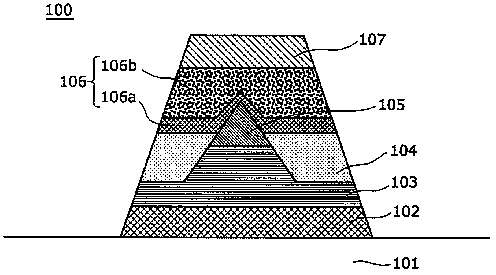
[0084] figure 1 It is a cross-sectional view showing a configuration example of the variable resistance element 100 according to Embodiment 1 of the present invention.

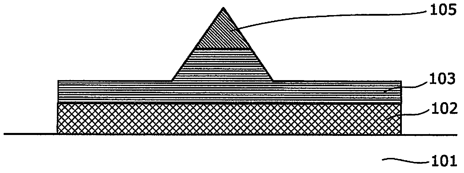
[0085] Such as figure 1 As shown, the variable resistance element 100 includes a substrate 101; an adhesive layer 102 (10-20 nm in thickness) formed on the substrate 101 and made of titanium nitride (TiN); formed on the adhesive layer 102, made of titanium aluminum nitride (TiAlN) truncated conical conductive layer 103 (thickness 50-100nm); conical (needle)-shaped second electrode 105 formed on the conductive layer 103; formed on the second electrode 105 covering the second electrode 105 The second variable resistance layer 106a (thickness 2-10nm); the interlayer insulating layer 104 formed on the conductive layer 103 and the second electrode 105 covering the conductive layer 103 and the part of the second electrode 105 excluding the needle-shaped part; ...

Embodiment approach 2

[0109] [Structure of variable resistance element]

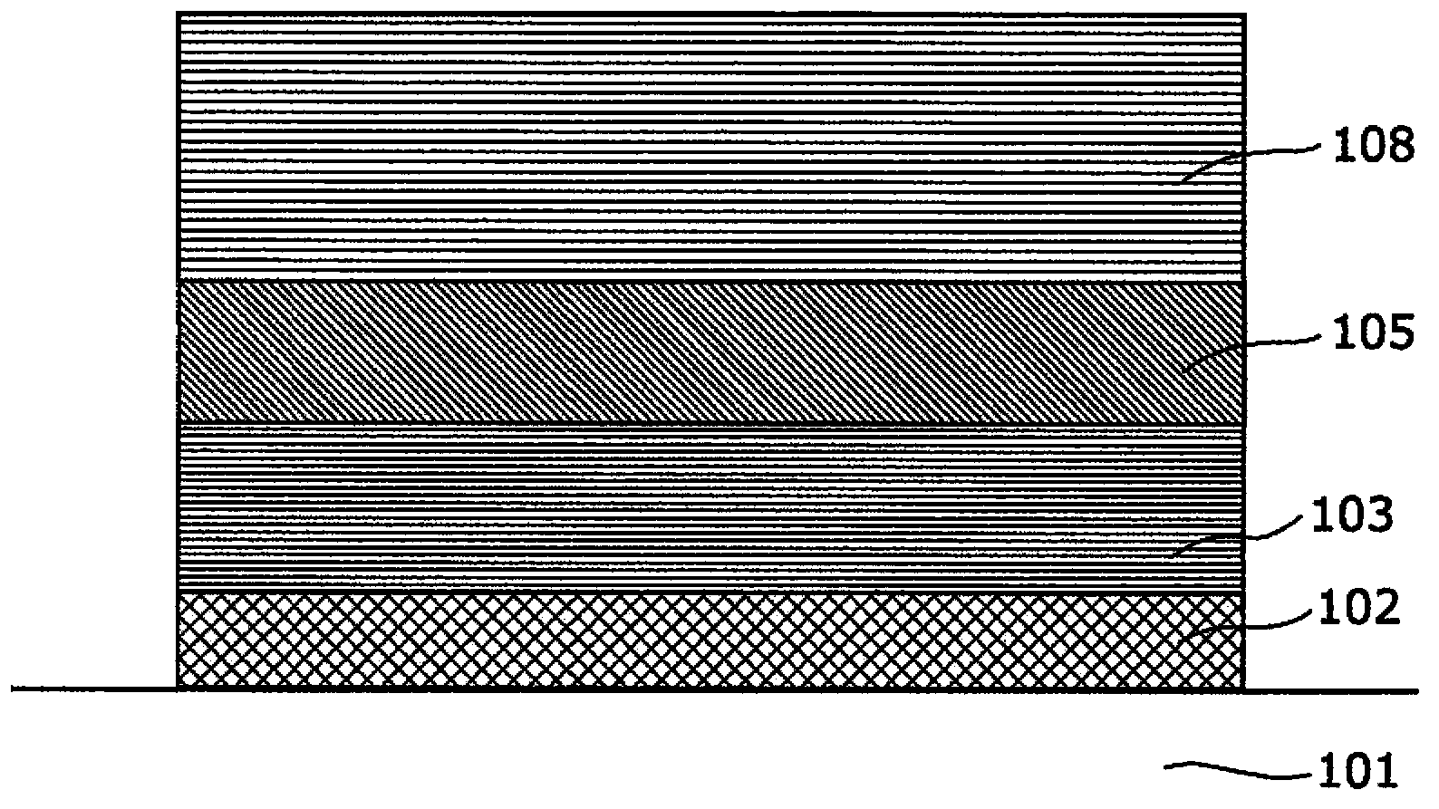
[0110] image 3 It is a cross-sectional view showing a configuration example of the variable resistance element 300 according to Embodiment 2 of the present invention.

[0111] Such as image 3 As shown, the variable resistance element 300 includes: a substrate 301; an adhesive layer 302 (10-20 nm in thickness) formed on the substrate 301 and made of titanium nitride (TiN); a first electrode 307 (5-100 nm in thickness), It is formed on the adhesive layer 302 and is composed of tantalum nitride (TaN); the first variable resistance layer 306b (thickness 18-95nm) is formed on the first electrode 307; the interlayer insulating layer 304 is formed on the adhesive layer 302, On the laminated structure composed of the first electrode 307 and the first variable resistance layer 306b and the substrate 301; a spacer (spacer) 309 is formed on the upper surface of the first variable resistance layer 306b that penetrates the interlayer ...


PUM


Abstract

A resistance change element has a first electrode (107), a second electrode (105), and a resistance change layer (106) provided interposed between the first and second electrodes (107, 105) so as to be in contact with the first and second electrodes (107, 105) and in which a resistance value reversibly changes on the basis of an applied electrical signal. The resistance change layer (106) is constituted by a layered structure of a first resistance change layer (106b) constituted by a first oxygen-deficient metal oxide, and a second resistance change layer (106a) constituted by a second transition metal oxide in which the degree of oxygen deficiency is lower than the degree of oxygen deficiency in the first resistance change layer (106b). The second electrode (105) has just one needle-shaped section at the interface with the second resistance change layer (106a), and the second resistance change layer (106a) is provided between the first resistance change layer (106b) and the second electrode (105) so as to be in contact with the first resistance change layer (106b) and the second electrode (105) and so as to cover the needle-shaped section.

Description

technical field [0001] The present invention relates to a resistance variable element, and more particularly to a resistance variable resistance element whose resistance value changes reversibly according to an applied electric signal, and a method for manufacturing the same. Background technique [0002] In recent years, with the advancement of digital technology for electrical equipment, there has been an increasing demand for large-capacity, non-volatile memory devices in order to store data such as music, images, and information. As a countermeasure to meet such demands, attention has been paid to nonvolatile memory devices (hereinafter referred to as ReRAM) that use a variable resistance element whose resistance value changes in response to an applied electrical signal in a memory cell and maintains that state continuously. . This is because the variable resistance element has features such as relatively simple structure, easy densification, and easy compatibility with...

Claims


Application Information

Patent Timeline
Patent Type & Authority Applications(China)
IPC IPC(8): H01L27/105H01L45/00H01L49/00
CPCH01L45/1253H01L45/146H01L45/1273H01L45/1675H01L45/1233H01L45/08H01L45/1625H01L45/16H10N70/24H10N70/8418H10N70/026H10N70/011H10N70/8833H10N70/063H10N70/826H10N70/841
Inventor 魏志强高木刚三谷觉川岛良男高桥一郎
Owner III HLDG 12 LLC
Why Eureka
Try Eureka