Acoustic surface wave filter device
A surface acoustic wave filtering and surface wave filter technology, which is applied to electrical components, impedance networks, etc., can solve problems such as the difficulty of reducing the size, the increase in the size of the surface acoustic wave filter device 500, and the increase in the cost of the surface acoustic wave filter device. , to achieve the effect of improving the phase balance
Inactive Publication Date: 2002-10-30
MURATA MFG CO LTD
1 Cites 3 Cited by
AI-Extracted Technical Summary
Problems solved by technology
Therefore, the size of the surface acoustic wave filter device 500 is significantly increased, making size reduction difficult.
In addition, due ...
Method used
As discussed above, by setting the ratio C2/C1 of the IDT total electrostatic capacitance value C2 of the surface acoustic wave filter element 102 to the IDT total electrostatic capacitance value C1 of the surface acoustic wave filter element 101 at the above-mentioned In the specified range discussed and the ratio GR2/GR1 of the interval GR2 from the IDT to the reflector and the interval GR1 from the IDT to the reflector is also set within the specified range discussed above, then the surface acoustic wave filter with unbalanced to balanced conversion function The balance of the device 100 can be effectively improved.
Equally, in the embodiment of the present invention, also can adopt the method that the impedance characteristic of surface acoustic wave filter element 101 and 102 depends on total IDT capacitance value to form surface acoustic wave filter device, by increasing surface acoustic wave The total electrostatic capacitance value of the plurality of IDTs 114 to 116 of the wave filter element 102 shifts the impedance characteristic of the surface acoustic wave filter element 102 to a low impedance, thereby eliminating the mismatched impedance between the surface acoustic wave filter elements 101 and 102 characteristic.
Fig. 5 has shown the IDT of a surface acoustic wave filter element and the relation between IDT interval and impedance characteristic, wherein, IDT and IDT interval are about 1.27 times with surface acoustic wave wavelength as base value and take half wavelength as Units increase. It can be seen from Figure 5 that the impedance characteristics of the surface acoustic wave filter components can be increased by increasing the IDT and IDT intervals.
It should be noted that the number of finger electrodes in each of the first and second surface acoustic wave filter elements 101 and 102 shown in FIG. 1 and the number of finger electrodes of the reflector are less than the actu...
Abstract
A surface acoustic wave filter device has a balanced to unbalanced conversion function, and the device has different input/output impedances and good balance in the pass band. The surface acoustic wave filter device has a balanced-to-unbalanced conversion function, and in this device, the interval of the input/output IDT of the second surface acoustic wave filter element is larger than that of the input/output IDT of the first surface acoustic wave filter element. spaced about half the wavelength of the surface acoustic wave so that the phase is reversed, wherein the total electrostatic capacitance value of the plurality of IDTs of the second surface acoustic wave filter element is greater than the total of the plurality of IDTs of the first surface acoustic wave filter element electrostatic capacitance value.
Application Domain
Impedence networks
Technology Topic
CapacitanceSurface wave +7
Image
Examples
- Experimental program(1)
Example Embodiment
[0058] With reference to the drawings, the present invention will be discussed in accordance with specific preferred embodiments of the surface acoustic wave filter device of the present invention.
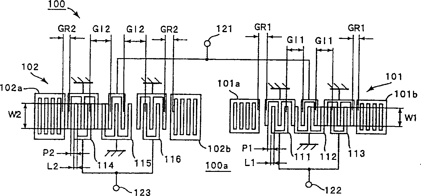
[0059] figure 1 It is a schematic plan view of a surface acoustic wave filter device according to the first preferred embodiment of the present invention.
[0060] By preparing such as on the piezoelectric substrate 100a figure 1 In the electrode structure shown, the first surface acoustic wave filter element 101 and the second surface acoustic wave filter element 102 are provided in the surface acoustic wave filter device 100. In this preferred embodiment, the first surface acoustic wave filter element 101 has the first IDT111 to the third IDT113 arranged along the surface acoustic wave transmission direction, and the second surface acoustic wave filter element 102 has the surface acoustic wave The first IDT114 to the third IDT116 are set in the transmission direction. In addition, in the first surface acoustic wave filter element 101, reflectors 101a and 101b are arranged on both sides of the three IDTs along the surface acoustic wave transmission direction, and in the second surface acoustic wave filter element 102, the reflectors The devices 102a and 102b are arranged on both sides of the three IDTs along the surface acoustic wave transmission direction.
[0061] One end of each IDT 112 near the center of the first surface acoustic wave filter element 101, that is, each first end, and one end of each IDT 115 near the center of the second surface acoustic wave filter element 102, that is, each first end are commonly connected together, and are connected together. The balanced input 121 is electrically connected. One ends of the respective IDTs 111 and 113 of the first surface acoustic wave filter element 101 are connected together to form a second end, and the second end is connected to the first balanced output end 122. In addition, the output ends of IDT 114 and 116 of the second surface acoustic wave filter element 102 are connected together to form a second end, and the second end is electrically connected to the second balanced output end 123.
[0062] The feature of this preferred embodiment is that the total electrostatic capacitance value of IDTs 114 to 116 of the second surface acoustic wave filter element 102 is greater than the total electrostatic capacitance value of IDTs 111 to 113 of the first surface acoustic wave filter element 101. Therefore, in the surface acoustic wave filter device 100 having a balanced to unbalanced conversion function, the amplitude balance and the phase balance can be greatly improved. This will be discussed with reference to specific experimental examples.
[0063] Piezo substrates can use LiTaO 3 Substrate. Alternatively, other piezoelectric single crystals or piezoelectric ceramics can also be used as the piezoelectric substrate.
[0064] The first and second surface acoustic wave filter elements 101 and 102 are prepared on a piezoelectric substrate.
[0065] It should be noted that figure 1 The number of finger electrodes shown in each of the first and second surface acoustic wave filter elements 101 and 102 and the number of finger electrodes of the reflector are smaller than the actual number, which is beneficial to simplify the description.
[0066] A specific example of the preferred embodiment is discussed below.
[0067] (1) First surface acoustic wave filter element 101
[0068] The crossing width of the finger electrode W1=128μm;
[0069] The number of pairs of finger electrodes in IDT: the number of pairs of finger electrodes of IDT112 near the center=17, and the number of pairs of finger electrodes of IDT111 and 113 on both sides=11;
[0070] The finger electrode pitch P1 in IDT111 to 113=2.10μm;
[0071] According to IDT L1/P1, the effective range of the electrode=0.72 (L1 refers to the width of the electrode);
[0072] The number of finger electrodes of reflectors 101a and 101b=120;
[0073] The finger electrode pitch PR of the reflectors 101a and 101b = 2.15 μm;
[0074] The interval GT1 between IDT and IDT in IDT111 to 113 is GT1=1.27λ, where λ represents the wavelength of the surface acoustic wave. In this specification, "IDT and IDT interval" is set as the distance between the center of the finger electrode that is closest to the adjacent IDT on the side of the signal electrode.
[0075] The interval between the IDT and the reflector GR1=0.500λ, and "the interval between the IDT and the reflector" is defined as the distance between the IDT and the center of the adjacent finger electrode of the reflector.
[0076] (2) Second surface acoustic wave filter element 102
[0077] Cross width W2=145μm;
[0078] Number of finger electrode pairs in IDT114 to 116: IDT115 finger electrode pairs near the center=17, IDT114 and 116 finger electrode pairs on both sides=17;
[0079] IDT114 to 116 finger electrode pitch P2=2.10μm;
[0080] According to IDT L2/P2, the effective range of the electrode=0.70 (L2 refers to the width of the electrode);
[0081] The number of finger electrodes of the reflectors 102a and 102b is NR=120;
[0082] The finger electrode pitch PR of the reflectors 102a and 102b = 2.15 μm;
[0083] The interval between IDT and IDT GT2 = 1.77λ;
[0084] The distance between IDT and reflector GR=0.494λ;
[0085] In the surface acoustic wave filter device 100 of the present preferred embodiment, the total electrostatic capacitance value of the surface acoustic wave filter element 101 IDT 111 to 113 is preferably about 3.0 pF, and the surface acoustic wave filter element 102 IDT 114 to 116 The total electrostatic capacitance value is preferably about 3.4pF.
[0086] In the surface acoustic wave filter element 100 of this preferred embodiment, the interval between IDT and IDT is different for the first surface acoustic wave filter element 101 and the second surface acoustic wave filter element 102, as described above Discussed. That is, since the interval between the IDT and IDT of the surface acoustic wave filter element 102 and the interval between the IDT and IDT of the surface acoustic wave filter element 101 differ by half a wavelength, the difference between the unbalanced input terminal 121 and the balanced output terminal 122 The transmission phase characteristic differs from the transmission phase characteristic between the unbalanced input terminal 121 and the balanced output terminal 123 by about 180°.
[0087] figure 2 with image 3 The frequency characteristics of the amplitude balance and the phase balance of the surface acoustic wave filter device 100 of the preferred embodiment are shown.
[0088] For comparison, Picture 20 with Figure 21 shown Figure 19 The frequency characteristics of the amplitude balance and the phase balance of the conventional surface acoustic wave filter device 500 are shown. figure 2 with image 3 versus Picture 20 with Figure 21 The comparison shows that, in the preferred embodiment, the amplitude balance in the band is about 0.5dB or less than 0.5dB and the phase balance in the band is about 4.9 degrees or less than 4.9 degrees, thereby satisfying the degree of balance.
[0089] The reasons why the above method is adopted to improve the degree of balance in this embodiment will be discussed in detail below.
[0090] In the surface acoustic wave filter device 100, an electric signal is input to the unbalanced input terminal 121, the electric signal is filtered in the respective surface acoustic wave filter elements 101 and 102, and the output signal is extracted from the balanced output terminals 122 and 123. Here, between the first surface acoustic wave filter element 101 and the second surface acoustic wave filter element 102, the above-discussed method is used to make the interval between IDT and IDT differ by half the wavelength of the surface acoustic wave. Therefore, the amplitude characteristics to be filtered are basically the same, while the phase characteristics of the transmission are opposite. Therefore, the amplitude characteristics of the electrical signals induced at the balanced output terminals 122 and 123 are basically the same, while the phase characteristics of the transmission are opposite.
[0091] In the three IDT-type cascaded resonant SAW filters of this embodiment, the classic method is to use Figure 4A The three resonant modes shown are used to generate the passband. in Figure 4A In order to facilitate the understanding of the resonance mode, the displayed frequency characteristics are measured in a state where the input/output impedance is intentionally set to be mismatched. The parts indicated by arrows A, B, and C are the resonance frequencies of the respective resonance modes.
[0092] Figure 4B The effective current density distribution of each resonance mode is shown. The response with the lowest frequency indicated by arrow B is called the "secondary mode", which is a resonance mode with two nodes within the effective current density distribution range.
[0093] The intermediate response indicated by arrow A is called the "zero-order mode", which is a resonance mode with no dots in the effective current density distribution range.
[0094] The response with the highest frequency indicated by arrow C is a standing wave resonance having a surface wave density distribution peak in the interval between IDT and IDT.
[0095] Regarding the three resonance modes discussed above, in the resonance mode A at the center of the band and the resonance mode C at the higher frequency of the band, since the effective current density of the surface acoustic wave in the interval between IDT and IDT is large, Therefore, increase the IDT and IDT interval. Therefore, this filter is very sensitive to interference when the area where the surface acoustic wave cannot be excited or received is large.
[0096] Since it is difficult to effectively excite and receive standing waves, high impedance characteristics are obtained.
[0097] Figure 5 The relationship between the IDT and IDT interval and impedance characteristics of a surface acoustic wave filter element is shown. The interval between IDT and IDT is about 1.27 times the surface acoustic wave wavelength as the base value and increased in units of half a wavelength. From Figure 5 It can be seen that by increasing the interval between IDT and IDT, the impedance characteristics of surface acoustic wave filter components can be increased.
[0098] The difference in impedance characteristics actually affects the reflection characteristics at the connection point, especially the amplitude balance. It is difficult to transmit signals to components with higher impedance or to transmit signals to components with lower impedance. Therefore, the difference in impedance characteristics will cause the amplitude balance to deteriorate.
[0099] Therefore, when the surface acoustic wave filter element 102 is constructed by increasing the interval between IDT and IDT by half the wavelength of the surface acoustic wave, the phase characteristic of the transmission is different from that of the surface acoustic wave filter element 101 by 180. When compared with the impedance characteristic of the first surface acoustic wave filter element 101, the impedance characteristic of the second surface acoustic wave filter element 102 changes toward a higher impedance, which causes the amplitude balance to deteriorate.
[0100] Similarly, in the embodiment of the present invention, a method in which the impedance characteristics of the surface acoustic wave filter elements 101 and 102 depend on the total IDT electrostatic capacitance value can also be used to form a surface acoustic wave filter device, by adding a surface acoustic wave filter The total electrostatic capacitance value of the plurality of IDTs 114 to 116 of the element 102 shifts the impedance characteristic of the surface acoustic wave filter element 102 to a low impedance, thereby eliminating the mismatched impedance characteristic between the surface acoustic wave filter elements 101 and 102.
[0101] Regarding the ratio C2/C1 of the total IDT capacitance value C2 of the surface acoustic wave filter element 102 and the total IDT capacitance value C1 of the surface acoustic wave filter element 101, when the total IDT value of the surface acoustic wave filter element 101 is When the electrostatic capacitance value C1 is used as a reference value and the total electrostatic capacitance value C2 of the IDT of the surface acoustic wave filter element 102 is used as a variable, the relationship between the capacitance value ratio C2/C1 can be determined.
[0102] Figure 6 with Figure 7 The relationship between the IDT total capacitance value ratio C2/C1 and the amplitude balance is shown, where the total electrostatic capacitance value C1 of IDT111 to 113 of the surface acoustic wave filter element 101 is fixed and the second surface acoustic wave filter element The total electrostatic capacitance value C2 of the IDT of 102 is variable. Can be from Figure 6 Seen in the middle: when the ratio C2/C1 is about 1.10, the amplitude balance is at the minimum value. When the ratio C2/C1 is in the range of about 1.0 to about 1.20, the amplitude balance is about 1.0dB or lower. Under the condition of 1.0dB.
[0103] Therefore, it can be seen that when the ratio C2/C1 is about 1.10, the amplitude balance reaches its minimum value, and when it is within the range of 1.00 <1.20, the amplitude balance is close to 1.0dB or less than 1.0dB.
[0104] The electrostatic capacitance value of IDT is proportional to the effective range of electrodes in IDT, the cross width of finger electrodes and the number of pairs of finger electrodes.
[0105] Therefore, in terms of the IDT electrode effective range M1 of the surface acoustic wave filter element 101, the finger electrode crossing width W1, and the total number of IDTs N1, when the surface acoustic wave filter element 102 IDT electrode effective range M2, the finger electrode crossing When the width W2 and the total number of IDT logarithms N2 are preferably within the range of M1×W1×N1 <1.20×M1×W1×N1, the total electrostatic capacitance of IDT is within the range discussed above , The amplitude balance and phase balance are greatly improved.
[0106] Since the effective range of the IDT electrode affects the transmission characteristics of surface waves, such as the speed of sound, the impact on the phase balance is large. The effective range of the electrode of the surface acoustic wave filter element 101 is made different from the effective range of the electrode of the surface acoustic wave filter element 102, and the change in the degree of phase balance can be detected. Picture 10 The change in the degree of phase balance related to the ratio M2/M1 of the electrode effective range M2 of the surface acoustic wave filter element 102 and the electrode effective range M1 of the surface acoustic wave filter element 101 is displayed. Wherein, the crossing width of the finger electrodes is set so that the ratio C2/C1 of the total electrostatic capacitance value of the IDT is within the range discussed above.
[0107] Just like Picture 10 As shown, when the ratio M2/M1 is in the range close to 0.97 to close to 1.0, the phase balance reaches a minimum. It can also be seen that the conditional range that satisfies the phase balance of about 10 degrees or less is within the range close to 0.93 <1.05.
[0108] On the other hand, in Figure 4A In the resonance mode B shown at the lower frequency of the passband, since the interval between IDT and IDT corresponds to the node of the effective current density distribution, the filter is not affected when the interval between IDT and IDT increases. However, when the electrostatic capacitance value of the IDT changes, its influence is similar to that of the other two resonance modes A and B.
[0109] In addition, when the IDT-to-reflector interval is changed, the resonance mode at lower frequencies in the passband is most affected. Therefore, by optimizing the ratio C2/C1 of the total electrostatic capacitance value and simultaneously optimizing the IDT-to-reflector interval GR1 of the surface acoustic wave filter element 101 and the IDT-to-reflector interval GR2 of the surface acoustic wave filter element 102, Can very effectively improve the balance.
[0110] Figure 8 with Picture 9 The relationship between the ratio GR2/GR1 and the amplitude balance and the relationship between the ratio GR2/GR1 and the phase balance under the condition of changing the IDT to reflector interval GR2 relative to the IDT to reflector interval GR1 are respectively shown.
[0111] From Figure 8 It can be seen that when the ratio GR2/GR1 is about 0.99, the amplitude balance is close to the lowest value, and the range that satisfies the amplitude balance of about 1.0dB or less than 1.0dB is 0.96 <1.02. In addition, from Picture 9 It can be seen that if the ratio GR2/GR1 is within this range, the phase balance is about 10 degrees or less.
[0112] Here, although it is preferable to use a grating type reflector as the reflector, the reflector is not limited to a grating type, and a reflector using reflection from a tip surface may be used.
[0113] As discussed above, by setting the ratio C2/C1 of the total IDT capacitance value C2 of the surface acoustic wave filter element 102 to the total IDT capacitance value C1 of the surface acoustic wave filter element 101 in the above-discussed designation And the ratio GR2/GR1 between the IDT to reflector interval GR2 and the IDT to reflector interval GR1 is also set within the specified range discussed above, then the surface acoustic wave filter device 100 with unbalanced to balanced conversion function The balance can be effectively improved.
[0114] Although in the preferred embodiment, three IDT-type cascaded resonant surface acoustic wave filter elements 101 and 102 are preferably used, in the present invention, the first and second surface acoustic wave filter elements are The number of IDTs is not limited to three IDT types, and a multi-electrode type cascaded resonant surface acoustic wave filter can also be used.
[0115] Picture 11 It is a schematic plan view showing the electrode structure of the surface acoustic wave filter device according to the second preferred embodiment of the present invention.
[0116] In this preferred embodiment, the electrode structure is prepared as in the first preferred embodiment LiTaO 3 The substrate is made of a piezoelectric substrate. Similar to the first preferred embodiment, the piezoelectric substrate can also be made of other piezoelectric single crystals or piezoelectric ceramics.
[0117] In this preferred embodiment, each first end of the first surface acoustic wave filter element 201 and the second surface acoustic wave filter element 202 is connected to the unbalanced input end 221. In addition, each output end of the first surface acoustic wave filter element 201 and the second surface acoustic wave filter element 202, that is, each second end, is connected to the balanced output ends 222 and 223, respectively. In addition, the surface acoustic wave filter elements 201 and 202 are constructed in the same manner as the surface acoustic wave filter elements 101 and 102 of the first preferred embodiment. That is, the surface acoustic wave filter element 201 has IDTs 211 to 213 arranged along the surface wave transmission direction, and the surface acoustic wave filter element 202 has IDTs 214 to 216 arranged along the surface wave transmission direction. In addition, reflectors 201a, 201b, 202a, and 202b are provided on both sides of the IDT along the surface wave transmission direction.
[0118] The unbalanced input terminal 221 is connected to the IDT 212 and 215 at a position close to the center. The balanced output terminal 222 is connected to IDT 211 and 213, and the balanced output terminal 223 is connected to IDT 214 and 216.
[0119] In the second preferred embodiment, at least one of the first and second surface acoustic wave filter elements 201 and 202, and the interval between at least one IDT and IDT is different from the interval between the other IDT and IDT and is different from that of the surface acoustic wave. Integer multiples of wavelength to improve balance. The discussion will now be based on specific experimental examples.
[0120] The structures of examples of the first and second surface acoustic wave filter elements 201 and 202 are as follows:
[0121] (1) First surface acoustic wave filter element 201
[0122] The crossing width of the finger electrode W1=125μm;
[0123] Number of IDT finger electrode pairs: IDT 212 finger electrode pairs near the center=17, IDT211 and 213 finger electrode pairs on both sides=11;
[0124] IDT's finger electrode pitch P1=2.1μm;
[0125] The effective range of the electrode L1/P1=0.70 (L1 refers to the width of the electrode);
[0126] The number of finger electrodes of the reflector NR=120;
[0127] The finger electrode pitch of the reflector PR = 2.15 μm;
[0128] The interval between IDT and IDT: in Picture 11 Where GT11=1.27λ and GT12=2.27λ;
[0129] The distance between IDT and reflector: GR1=0.500λ.
[0130] (2) Second surface acoustic wave filter element 202
[0131] The crossing width of the finger electrode W2=128μm;
[0132] Number of IDT finger electrode pairs: IDT115 finger electrode pairs near the center=17, IDT214 and 216 finger electrode pairs on both sides=11;
[0133] IDT's finger electrode pitch P2=2.1μm;
[0134] The effective range of the electrode L2/P2=0.70 (L2 refers to the width of the electrode);
[0135] The number of finger electrodes of the reflector NR=120;
[0136] The finger electrode spacing of the reflector λR = 2.15 μm;
[0137] The interval between IDT and IDT: in Picture 11 In, GT21=1.77λ and GT22=1.77λ;
[0138] The distance between IDT and reflector GR2=0.498λ, where λ represents the wavelength of the surface acoustic wave to be excited.
[0139] Picture 12 Shows the frequency characteristics of the amplitude balance of the surface acoustic wave filter device 200 of the preferred embodiment, and, Figure 13 The frequency characteristics of the phase balance of the surface acoustic wave filter device 200 of the preferred embodiment are shown. Picture 12 with Figure 13 And show the characteristics of the conventional example discussed above Picture 20 with Figure 21 In comparison, the results show that the phase balance in the band using the conventional method is about 4.4 degrees or less than 4.4 degrees, while in the preferred embodiment, the phase balance is about 5.0 degrees or less than 5.0 degrees. These are basically identical. However, when comparing the amplitude balance, the amplitude balance using the conventional method increases to 0.96 dB, while in the preferred embodiment, the amplitude balance is only about 0.19 dB or less than 0.19 dB.
[0140] The reasons will be discussed in more detail below.
[0141] Similarly, in the surface acoustic wave filter device 200, the electrical signal input to the unbalanced input terminal 221 is filtered by the surface acoustic wave filter elements 201 and 202, and its output signals are provided at the balanced output terminals 222 and 223. The electrical signal input to the surface acoustic wave filter element 202 is converted into a surface acoustic wave by the IDT215 and excited to generate a standing wave. The standing waves generated by the excitation are converted into electrical signals by IDT214 and 216. The signal to be transmitted is selected according to the frequency characteristics of the resonant mode of the standing wave to be excited, and the filtering discussed above can be completed.
[0142] Similarly, the electrical signal input to the surface acoustic wave filter element 201 is converted into a surface acoustic wave by the IDT212, and is excited to generate a standing wave. The standing waves generated by the excitation are converted into electrical signals by IDT211 and 213. At the same time, the transmitted signal is selected according to the frequency characteristics of the standing wave resonance mode to be excited, and the filtering discussed above can be completed.
[0143] In the surface acoustic wave filter element 201, the interval GI11 between the IDT and the IDT is different from the interval GI12 between the IDT and the IDT, and the difference is one wavelength of the surface acoustic wave. Therefore, the transmission phase characteristics of the signals sensed in IDT 211 and 213 are almost equal.
[0144] As discussed above, both the first and second surface acoustic wave filter elements 201 and 202 have the performance that increasing the interval between IDT and IDT will cause the impedance characteristic to increase. Even if the interval between multiple IDTs and IDTs only increases some of the intervals between IDTs and IDTs, the impedance will increase. However, the change in impedance characteristics at this time is much smaller than the change when all IDT and IDT intervals are increased.
[0145] In the surface acoustic wave filter device 200 of the preferred embodiment, the surface acoustic wave filter device 201 has only two different IDT and IDT intervals. Therefore, the impedance characteristic has a value when the interval between the two IDTs and IDT is small (for example, about 1.27λ) and the interval between the two IDTs and IDT is large (for example, about 2.27λ) The value between the impedance characteristics at the time. Just like Figure 5 As expected, this intermediate value corresponds to the impedance characteristic when the interval between the two IDTs and IDT is approximately 1.77λ, and matches the impedance characteristic of the surface acoustic wave filter element 202.
[0146] In addition, the intervals GI11 and GR12 between IDT and IDT in the surface acoustic wave filter element 201 are different from the intervals GI21 and GR22 between IDT and IDT in the surface acoustic wave filter element 202, and the difference is half the wavelength of the surface acoustic wave. Therefore, the phase of the transmission phase characteristic of the signal sensed at the balanced output terminal 222 differs from the phase of the transmission phase characteristic of the signal sensed at the balanced output terminal 223 by 180 degrees.
[0147] Therefore, the surface acoustic wave filter elements 201 and 202 have the performance that the transmission phase characteristics differ by 180 degrees, and the reason is that the interval between the IDT and the IDT differs by half a wavelength. In addition, since the surface acoustic wave filter elements 201 and 202 have the same impedance characteristics, the difference in amplitude balance between the signal sensed at the balanced output terminal 222 and the signal sensed at the balanced output terminal 223 is reduced.
[0148] The third preferred embodiment is an improvement of the surface acoustic wave filtering device 100 of the first preferred embodiment. Such as Figure 14 As shown, the surface acoustic wave resonators 304 and 304 are connected to one side of the unbalanced input terminal 121, and the surface acoustic wave resonators 306 and 306 are connected to one side of the balanced output terminals 122 and 123. Ignore the discussion of other features, and take the discussion of the first preferred embodiment as a reference.
[0149] More specifically, the surface acoustic wave resonator 304 is connected between the unbalanced input terminal 111 and the first end of the first surface acoustic wave filter element 101, and the other surface acoustic wave resonator 304 is connected between the unbalanced input terminal 111 and the first end of the first surface acoustic wave filter element 101. Between the input end 111 and the first end of the second surface acoustic wave filter element 102. In addition, the surface acoustic wave resonator 306 is connected between the second end of the first surface acoustic wave filter element 101 and the balanced output terminals 112 and 113, and the other surface acoustic wave resonator 306 is connected to the second surface acoustic wave. Between the second end of the wave filter element 102 and the balanced output ends 112 and 113.
[0150] The structures of examples of surface acoustic wave resonators 304 and 306 are as follows:
[0151] (1) Surface acoustic wave resonator 304
[0152] The crossing width of the finger electrode W=88μm;
[0153] The number of pairs of IDT finger electrodes N=80;
[0154] IDT's finger electrode pitch PI=2.10μm
[0155] The number of finger electrodes of the reflector NR=120;
[0156] Substrate is LiTaO 3.
[0157] (2) Surface acoustic wave resonator 306
[0158] The crossing width of the finger electrode W=80μm;
[0159] IDT's finger electrode number N=80;
[0160] IDT's finger electrode path PI = 2.12 μm
[0161] The number of finger electrodes of the reflector NR=120;
[0162] Substrate is LiTaO 3.
[0163] The attenuation frequency characteristic of the surface acoustic wave filter device 300 of the third preferred embodiment is as follows Figure 15 Shown by the solid line in. For comparison purposes, the attenuation frequency characteristic of the first preferred embodiment is Figure 15 The dashed line in shows. From Figure 15 It can be seen that the surface acoustic wave resonators 304 and 306 are connected in series on the side of the unbalanced input terminal 121 and the side of the first balanced output terminal 122 and 123 respectively, which increases the out-of-band attenuation, especially for higher frequencies in the passband. The attenuation increases.
[0164] Figure 16 It is a schematic plan view showing the electrode structure of the surface acoustic wave filter device according to the fourth preferred embodiment of the present invention.
[0165] In the surface acoustic wave filter device of the fourth preferred embodiment, on one side of the unbalanced input end of the surface acoustic wave filter device 200 of the second preferred embodiment, three IDTs 403a to 403c and the acoustic device having reflectors 403d and 403e The surface wave resonance filter 403 is connected. The rest of the structure is the same as that of the second preferred embodiment.
[0166] In the fourth preferred embodiment, since the surface acoustic wave resonator filter 403 is connected to the unbalanced input terminal 221 on one side, the attenuation of the higher frequency of the passband is increased. This will be discussed with reference to specific experimental examples.
[0167] This structure is basically the same as that of the second preferred embodiment. However, the design of the SAW resonator filter 403 is as follows:
[0168] The crossing width of the finger electrode W3=240μm;
[0169] IDT logarithm: IDT 403b finger electrode pairs close to the center=17, IDT 403a and 403c on both sides of each finger electrode pair=11;
[0170] IDT 403a to 403c finger electrode pitch P3=2.1μm;
[0171] The effective range of the electrode L3/P3=0.72 (L3 refers to the electrode width);
[0172] The number of finger electrodes of reflectors 403d and 403e is NR=120;
[0173] The finger electrode pitch PR of the reflectors 403d and 403e = 2.15 μm;
[0174] The interval between IDT and IDT GI=1.27λ;
[0175] The distance from IDT to reflector GR = 0.500λ;
[0176] Substrate is LiTaO 3.
[0177] Figure 17 The solid line in shows the attenuation frequency characteristic of the surface acoustic wave filter device of the fourth preferred embodiment, which is connected to the surface acoustic wave resonant filter 403 having the structure discussed above. For comparison purposes, Figure 17 The broken line in shows the attenuation frequency characteristic of the surface acoustic wave filter device of the second preferred embodiment. From Figure 17 It can be seen that according to the fourth preferred embodiment, the attenuation of higher frequencies in the passband is increased.
[0178] Figure 18 It is a schematic plan view illustrating a communication device 160 including a surface acoustic wave filter device according to various preferred embodiments of the present invention.
[0179] in Figure 18 Here, the duplexer 162 is connected to the antenna 161. The surface acoustic wave filter 164 and the amplifier 165 are called an RF (Radio Frequency) stage, and are connected between the duplexer 162 and the mixer 163 on the receiving side. In addition, a surface acoustic wave filter 169 of IF (Intermediate Frequency) stage is connected to the mixer 163. In addition, the amplifier 167 and the surface acoustic wave filter 168 are called an RF stage, and are connected between the duplexer 162 and the mixer 166 on the transmitting side.
[0180] The surface acoustic wave filters constructed according to various preferred embodiments of the present invention are suitable for the surface acoustic wave filters 164 and 168 in the communication device 160.
[0181] In the above discussion of the preferred embodiments of the present invention, it should be understood that any changes and improvements made by any person skilled in the art have not deviated from the core scope and basic spirit of the present invention. Therefore, the core scope of the present invention will be fully confirmed by the following claims.
PUM


Description & Claims & Application Information
We can also present the details of the Description, Claims and Application information to help users get a comprehensive understanding of the technical details of the patent, such as background art, summary of invention, brief description of drawings, description of embodiments, and other original content. On the other hand, users can also determine the specific scope of protection of the technology through the list of claims; as well as understand the changes in the life cycle of the technology with the presentation of the patent timeline. Login to view more.