Image quality tester of electronic display device

A technology for electronic displays and inspection devices, which can be used in measuring devices, televisions, instruments, etc., and can solve problems such as image quality inspection obstacles and high prices

Inactive Publication Date: 2003-04-02
KOKUSA ELECTRIC CO LTD
View PDF0 Cites 13 Cited by
  • Summary
  • Abstract
  • Description
  • Claims
  • Application Information

AI Technical Summary

Problems solved by technology

For this reason, when the light-emitting surface of the plasma display 1 is captured by a video camera having a resolution equivalent to that of the plasma display, as shown in FIG. Figure 4 As shown, moiré fringes (interference fringes) occur, and it is difficult to distinguish them from unsensitized pixels such as black spots.
[0006] In order to eliminate this moiré phenomenon, it is necessary to use a camera with a higher resolution than the number of pixels displayed on the monitor, or consider using a camera that uses a piezoelectric element to move the CCD element by half a pixel while taking pictures. The resolution is increased from the captured image, but in this method, the number of pixels increases with the increase in resolution, and it is necessary to separate non-luminous parts such as spacers and electrodes from black spots. , which requires an expensive high-speed image processing device

Method used


Image

  • Image quality tester of electronic display device
  • Image quality tester of electronic display device
  • Image quality tester of electronic display device

Examples


Embodiment Construction

[0021] Embodiment of the invention

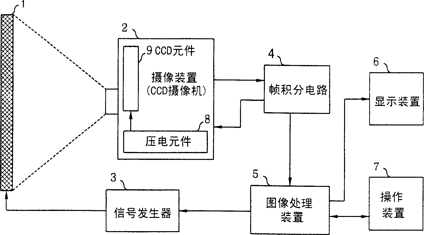
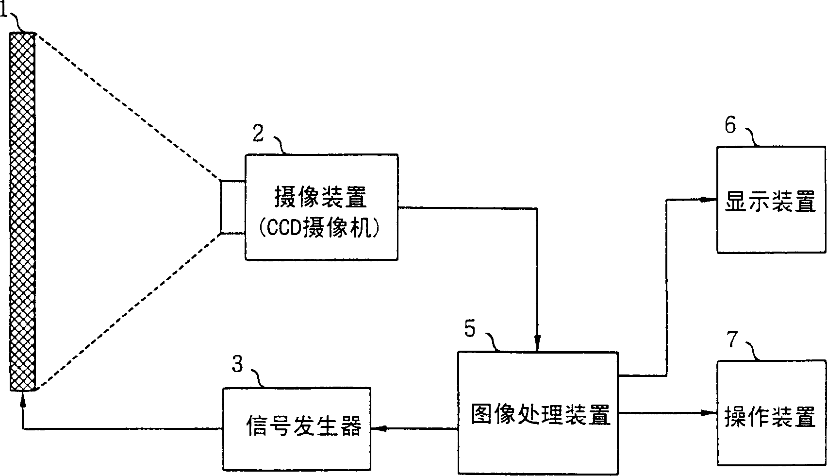
[0022] Below, refer to figure 1 An example in which the present invention is applied to a plasma display image quality inspection device will be described.

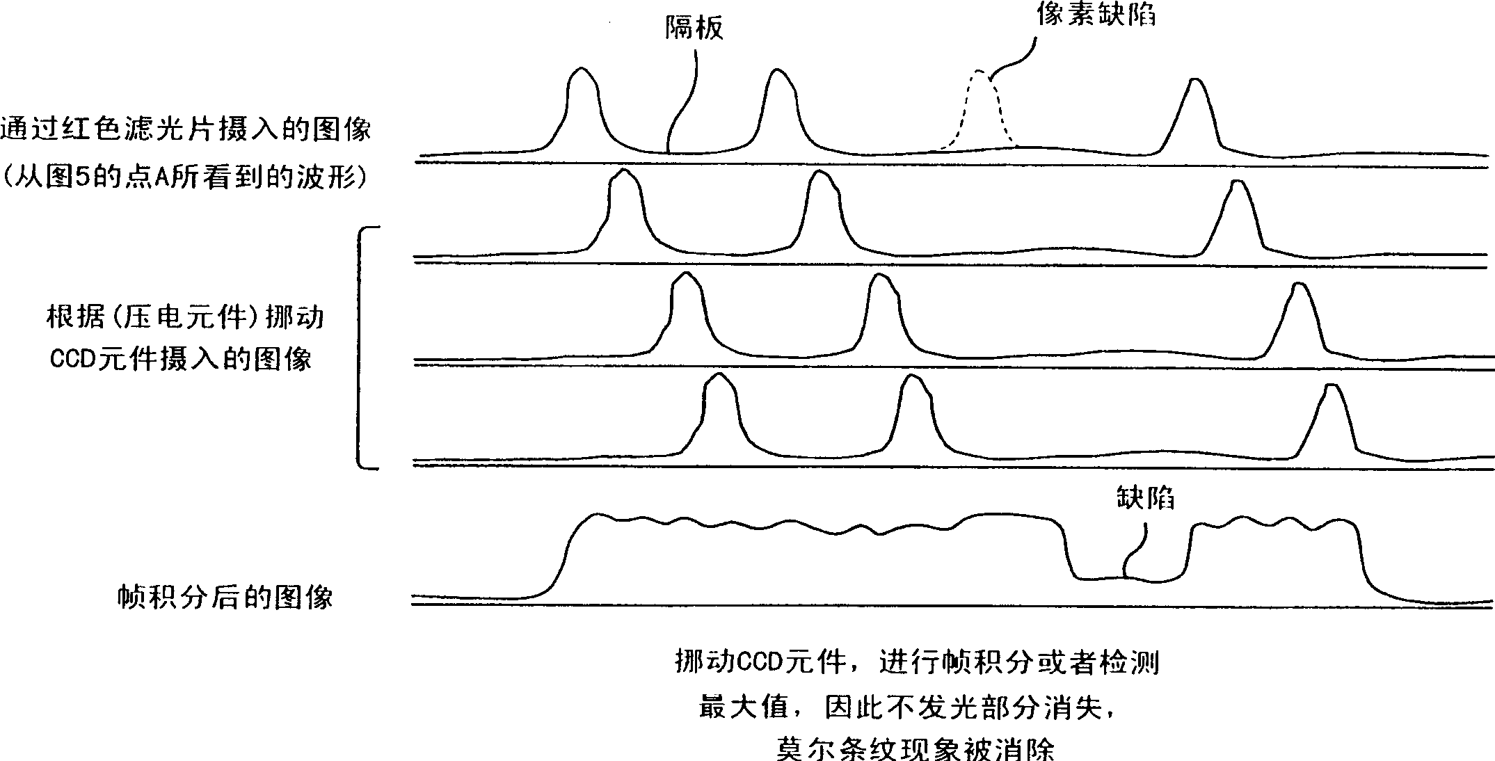
[0023] 1 is an electronic display device such as a plasma display, 2 is an imaging device such as a CCD camera, 3 is a signal generator for displaying images on a plasma display, and 4 is a frame integration circuit or a maximum value detection and holding circuit, for example, composed of a frame memory. If it is a frame integration circuit, each time a frame of image is read, the following action is repeated, that is, each pixel of the captured image and the image stored in the frame memory is integrated. If it is a maximum value detection and holding circuit, when each frame of image is read in, the following actions are repeated, that is, each pixel of the captured image is compared with the image stored in the frame memory, and then the higher-level In case it is updated to sto...


PUM


Abstract

This invention provides an image quality inspection apparatus that can easily eliminate moire caused by an unemission part such as a barrier and an electrode or the like in a display device such as a plasma display device without using a high definition CCD camera and a high-speed image processor so as to detect a pixel defect such as a black point (unemitted pixel) or the like at a high-speed. The electronic display image quality inspection apparatus for imaging an electronic display screen to inspect a defect caused in pixels of an electronic display device by using the image, is provided with a means that moves an imaging element photographing the electronic displays screen by a prescribed distance in longitudinal and lateral directions, a means that integrates the image photographed by each movement in terms of frames, and a means that inspects a pixel defect of the electronic display device from the image whose frames are integrated.

Description

technical field [0001] The invention relates to an electronic display image quality inspection device, which can automatically inspect display defects of electronic display devices such as plasma displays. Background technique [0002] As an example of conventional technology, a plasma display image quality inspection device using a CCD (charge-coupled device) camera is shown in image 3 , as explained below. [0003] 1 is an electronic display device such as a plasma display, 2 is an imaging device such as a CCD camera, 3 is a signal generator for displaying an image on a plasma display, and 5 is image processing for inspecting pixel defects from a captured image on a plasma display screen Device, 6 is the display device of the color monitor of displaying or printing inspection result, printer, 7 is the operation device of this inspection device. [0004] In the past, such as image 3 As shown, the signal generator 3 outputs a white display pattern on the entire display sc...

Claims


Application Information

Patent Timeline
Patent Type & Authority Applications(China)
IPC IPC(8): H04N13/02G01R31/00H04N17/00
CPCH04N5/21H04N17/004H04N17/04
Inventor 渡贯明男
Owner KOKUSA ELECTRIC CO LTD
Why Eureka
Try Eureka