Drive circuit of power semiconductor element

A technology of power semiconductors and drive circuits, which is applied to semiconductor devices, output power conversion devices, circuits, etc., and can solve problems such as longer time

Inactive Publication Date: 2003-10-01
MITSUBISHI ELECTRIC CORP
View PDF1 Cites 54 Cited by
  • Summary
  • Abstract
  • Description
  • Claims
  • Application Information

AI Technical Summary

Problems solved by technology

According to this, by clamping the gate potential to the breakdown voltage of the Zener diode and the breakdown voltage of the diode, the time until the IGBT is destroyed becomes longer at the time of overcurrent

Method used


Image

  • Drive circuit of power semiconductor element
  • Drive circuit of power semiconductor element
  • Drive circuit of power semiconductor element

Examples


Embodiment 1

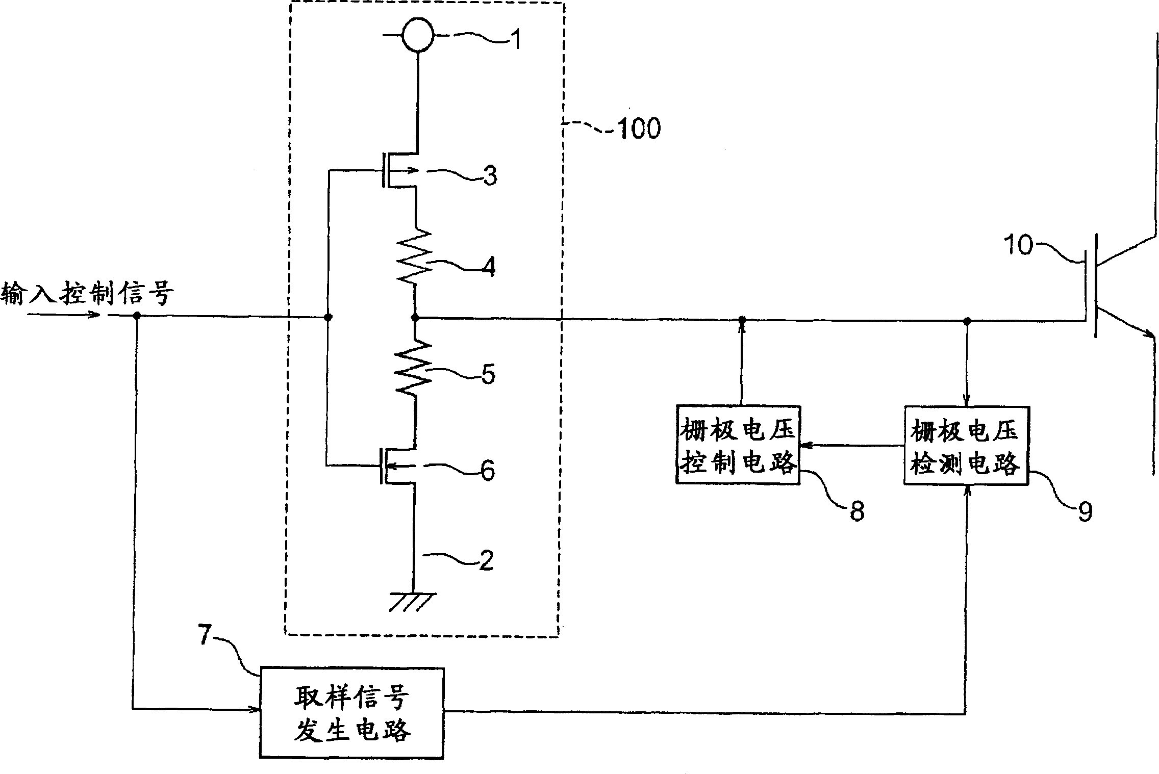
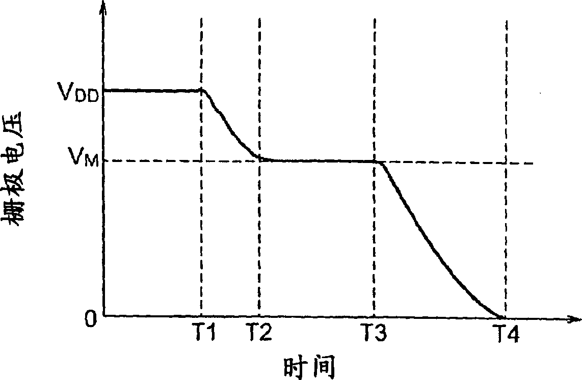
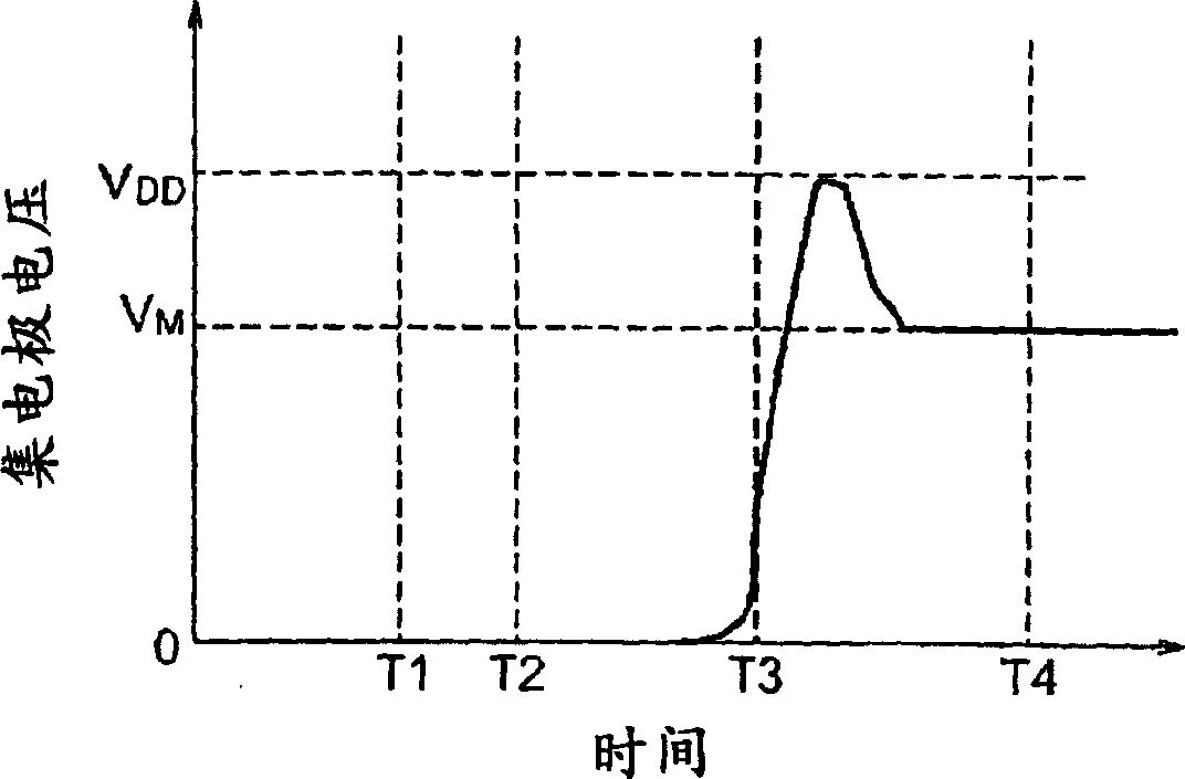
[0042] In order to suppress the occurrence of surge voltage, the present invention can adjust the gate voltage waveform when the current is cut off according to the current value flowing on the power semiconductor element. Therefore, in order to estimate the current value of the power semiconductor element, it is possible to detect the gate voltage (Miller voltage) of the semiconductor power element when it is turned off. The detection timing can also be adjusted with an input control signal through the sampling signal generating circuit.

[0043] figure 1 is a circuit diagram showing the configuration of a drive circuit for a power semiconductor element according to Embodiment 1 of the present invention. exist figure 1Among them, 100 is the main inverter circuit for on / off switching of the power semiconductor element; 7 is a sampling signal generating circuit that generates a sampling signal only when it is turned off with reference to the signal from the input control sign...

Embodiment 2

[0060] As an example of the configuration of the sampling signal generating circuit 7 of the first embodiment, there is a method using an ASIC. In this case, arbitrary waveforms can be generated. For example, when the input control signal 90 (solid line) indicated by the solid line in FIG. 5 is input to the driver, the gate voltage 91 becomes as shown by the dotted line in FIG. 5 . The circuit of the present invention can only work in shutdown, so the ASIC output Image 6 The waveform shown will do.

[0061] Also in this embodiment, the same effect as that of the first embodiment described above can be obtained.

Embodiment 3

[0063] Figure 7 An example of the sampling signal generating circuit 7 different from that of the second embodiment described above is shown. exist Figure 7 Among them, 11 is a resistor, 12 is a capacitor, 13 is a buffer, and 14 is a node. like Figure 7 As shown, the resistor 11 is set on the input side of the input control signal, and the buffer 13 is set on the side of the gate voltage detection circuit 9 . A resistor 11 is connected to a buffer 13, and to a capacitor 12 between a node 14 disposed therebetween and a ground point. Because the resistor 11 and the capacitor 12 form a low-pass filter, once the input control signal shown in Figure 5 is input, the voltage 93 (dotted line) of the node 14 produces the passivation waveform shown in Figure 8 (that is, the change point changes slowly waveform). Here, the threshold voltage of buffer 13 is half of the input: V DD / 2, by inputting the voltage generated by the node 14 into the buffer, the rectangular wave 92 shown...


PUM


Abstract

Provided is a drive circuit for a power semiconductor element capable of suppressing a surge voltage that occurs at the time of shutdown in an overcurrent state. The circuit includes: detecting that the input control signal indicates disconnection, and outputting a sampling signal generating circuit 7 of a sampling signal at the beginning of the Miller period of the IGBT10; The gate voltage detection circuit 9 that outputs an overcurrent detection signal in the above, and the gate voltage control circuit 8 that receives the overcurrent detection signal and controls the gate voltage of the IGBT 10 so that the IGBT 10 is turned off at a slower speed than usual.

Description

technical field [0001] The present invention relates to a drive circuit for power semiconductor elements, in particular to a drive circuit for driving power semiconductor elements such as IGBTs, that is, a drive circuit for power semiconductor elements used to suppress surge voltage generated during switching. Background technique [0002] Next, a conventional overcurrent protection method for an IGBT of a power semiconductor element will be described. When an overcurrent flows through the IGBT, use a comparator to compare the gate potential of the IGBT with the reference voltage. Only when the gate-emitter voltage of the IGBT rises higher than the reference voltage, the comparator works to turn on the switch. According to this, by clamping the gate potential to the breakdown voltage of the Zener diode and the breakdown voltage of the diode, the time until the IGBT is destroyed at the time of overcurrent becomes longer. In addition, through the operation of the monostable m...

Claims


Application Information

Patent Timeline
Patent Type & Authority Applications(China)
IPC IPC(8): H02M1/00H02M1/08H03K17/0812H03K17/16
CPCH03K17/08128H03K17/168H01L2924/0002H01L2924/00
Inventor 中山靖大井健史橋戶隆一
Owner MITSUBISHI ELECTRIC CORP
Why Eureka
Try Eureka