

Field electrode metal semiconductor field effect transistor
A technology of transistors and conductors, applied in the field of gallium arsenide field effect transistors, which can solve problems such as limiting the conduction state or maximum current
- Summary
- Abstract
- Description
- Claims
- Application Information
AI Technical Summary
Problems solved by technology
Method used
Image

Examples
Embodiment Construction
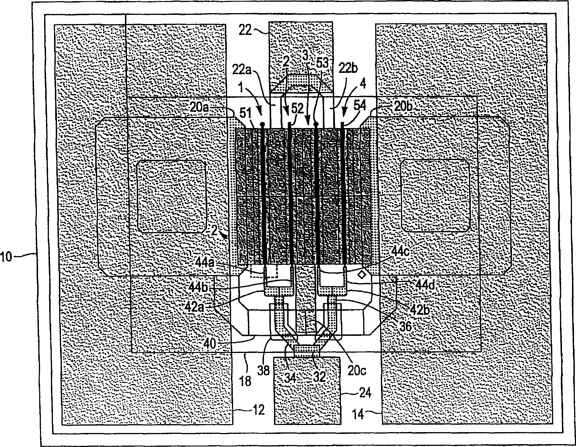
[0021] figure 1 is a plan view of a planar transistor according to an aspect of the present invention. exist figure 1 In , the chip on which the FET 8 is mounted is denoted by reference numeral 10, and areas 12 and 14 denote ground potential planes for on-wafer microwave measurements. In regions 12 and 14 , metallization 20 a , 20 b , 20 c represent source conductors, which are electrically connected in parallel by conductive vias shown at 40 . exist figure 1 Among them, the drain electrode, contact or bonding pad is represented by reference numeral 22, and the gate electrode, contact or bonding pad is represented by reference numeral 24.
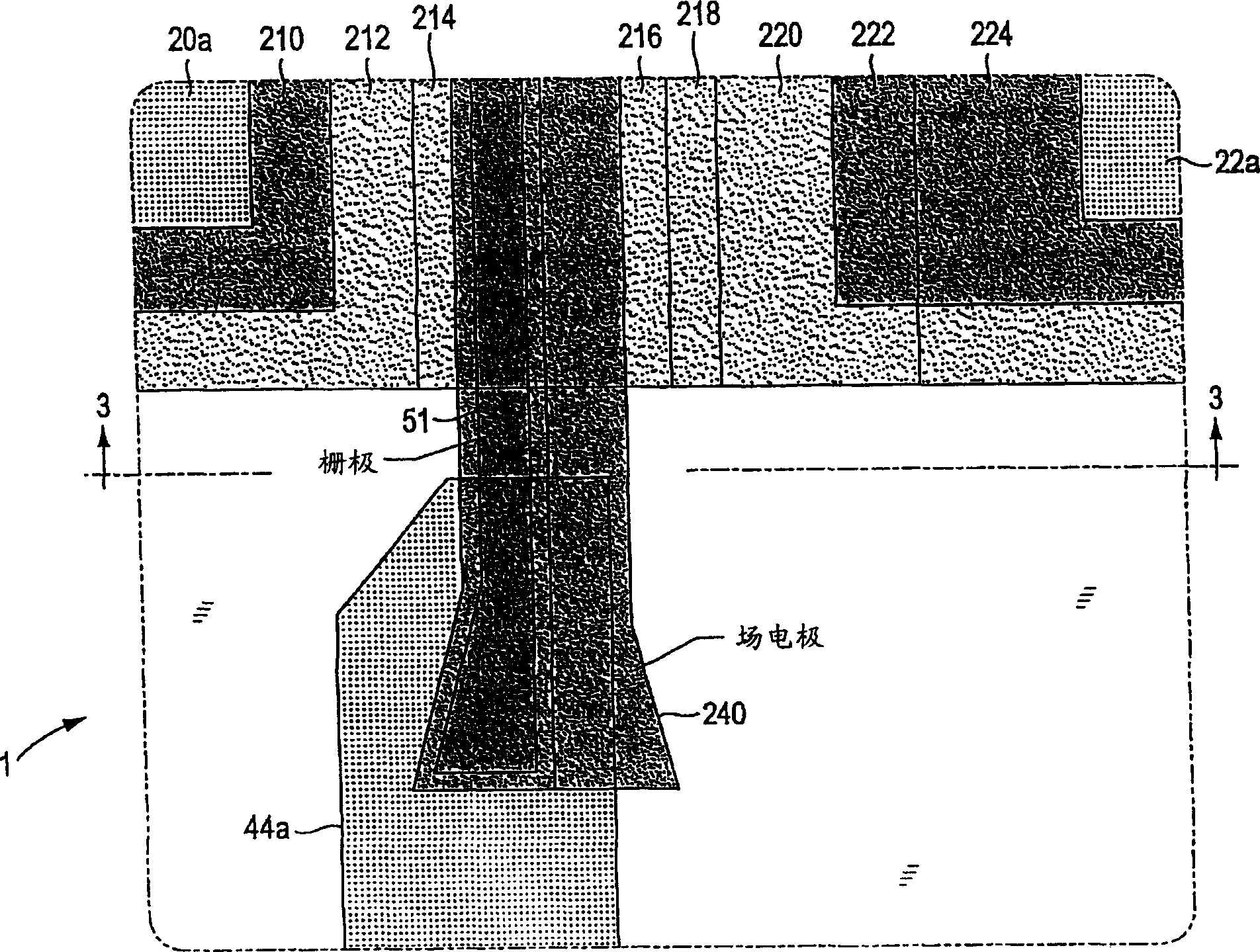
[0022] figure 1 The FET8 has four parallel independent FET elements, which are indicated by reference numerals 1, 2, 3 and 4, respectively. refer to image 3 These individual FET elements are described in detail.
[0023] exist figure 1 Among them, the drain pad 22 is connected to the drain region of the FET8 through metallization 2...
PUM
 Abstract
Description
Claims
Application Information