Active organic LED display and its making method

A technology of light-emitting diodes and manufacturing methods, applied in semiconductor/solid-state device manufacturing, instruments, electric solid-state devices, etc., can solve problems such as difficult driving circuit testing or repairing, and achieve high-intensity effects

Inactive Publication Date: 2004-07-28
AU OPTRONICS CORP
View PDF0 Cites 1 Cited by
  • Summary
  • Abstract
  • Description
  • Claims
  • Application Information

AI Technical Summary

Problems solved by technology

[0011] The object of the present invention is to provide an active organic light emitting diode display and its manufacturing method, so as to improve the shortcomings of the known method that it is difficult to test or repair the driving circuit because the driving circuit is formed inside the package cover.

Method used


Image

  • Active organic LED display and its making method
  • Active organic LED display and its making method
  • Active organic LED display and its making method

Examples


Embodiment Construction

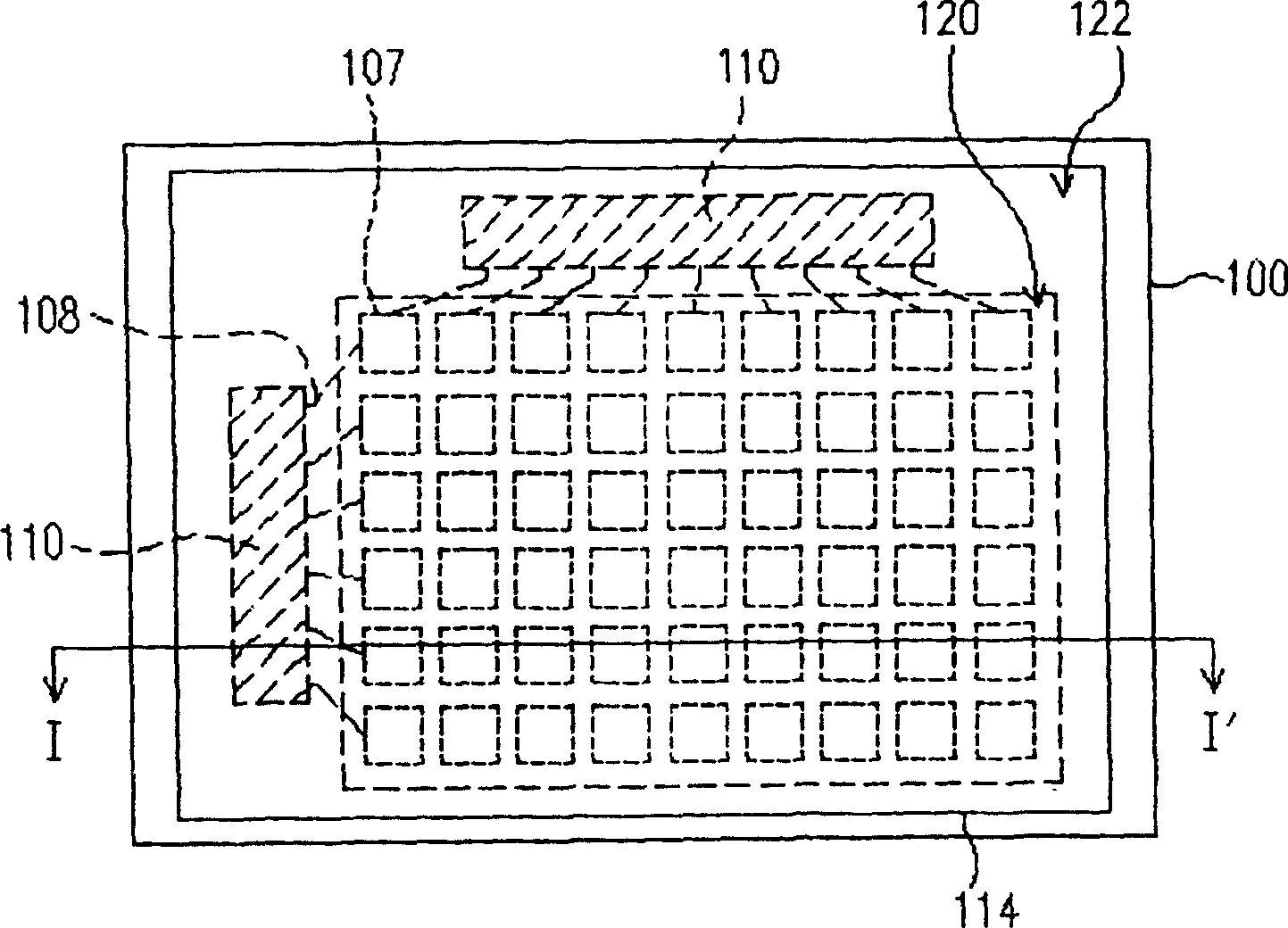
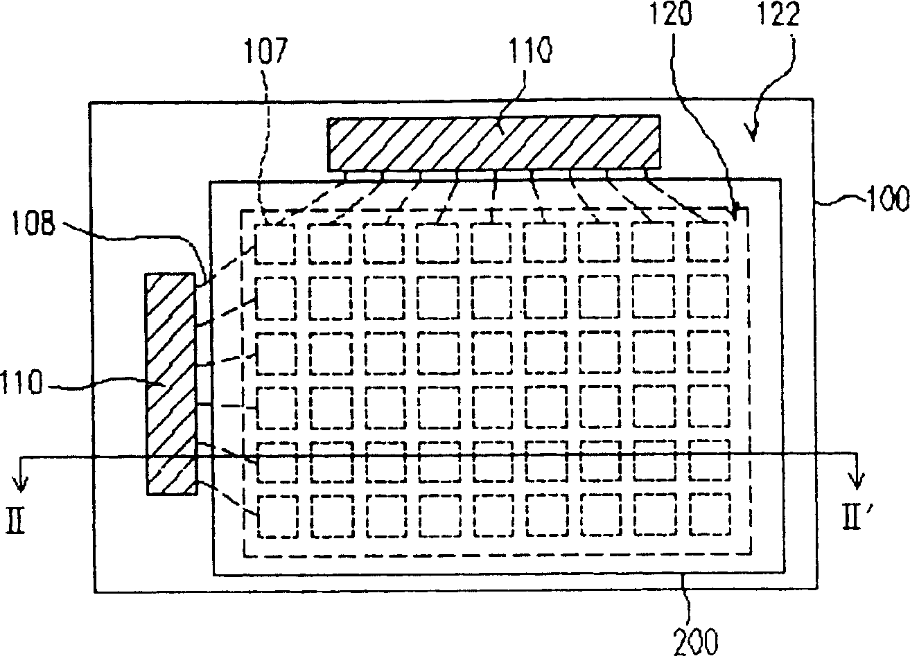
[0039] image 3 is a schematic top view of an active organic light emitting diode display according to a preferred embodiment of the present invention; Figure 4 for image 3 Schematic sectional view from II-II'.

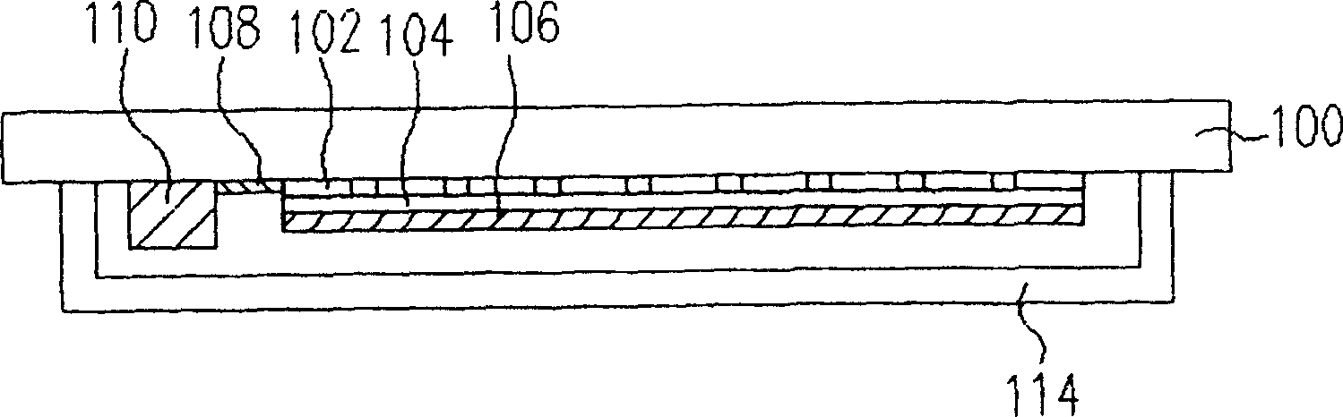
[0040] Please also refer to image 3 and Figure 4 The manufacturing method of the active organic light emitting diode display of the present invention is to firstly provide a substrate 100, wherein the substrate 100 has a light emitting region 120 and a non-light emitting region 122, and the light emitting region 120 of the substrate 100 has formed several arrays Pixel structures 107 , wherein each pixel structure 107 includes an active device and an anode layer 102 , a light emitting layer 104 and a cathode layer 106 .

[0041] Here, the active device in the pixel structure 107 is composed of at least two thin film transistors. In this embodiment, the active element is composed of two thin film transistors, one of which is responsible for switching and the ot...


PUM


Abstract

The invention relates to an active organic LED display making method, firstly providing a base plate with a luminous region and a nonluminous region, pixel structure formed in the light region; then forming a drive circuit in the nonluminous region, the drive circuit connected with the pixel structure; then setting a cap above the base plate and gluing the cap on the base plate, wherein the cap covers the luminous region and exposes the drive circuit. It can directly test or repair the drive circuit.

Description

technical field [0001] The present invention relates to a flat panel display and its manufacturing method, and in particular to an active matrix organic light emitting diode (Active Matrix Organic Light Emitting Diode, AMOLED) display and its manufacturing method. Background technique [0002] An organic light-emitting diode is a photoelectric element that can convert electrical energy into light energy and has high conversion efficiency. Its common applications are indicator lights, display panels, and the like. Due to the characteristics of organic light-emitting diode devices, such as no viewing angle, simple manufacturing process, low cost, high response speed, wide operating temperature range and full color, etc., which meet the requirements of display characteristics in the multimedia era, it has become a research boom in recent years. [0003] An active organic light emitting diode is currently under active development. An organic light emitting layer and a cathode la...

Claims


Application Information

Patent Timeline
Patent Type & Authority Applications(China)
IPC IPC(8): G09F9/30H01L27/15H01L27/32H01L51/56
Inventor 利锦洲宋志峯
Owner AU OPTRONICS CORP
Why Eureka
Try Eureka