Radioactive rays camera apparatus and radioactive rays camera system

A technology of radiography and radiation, applied in the fields of radiography devices and radiography systems, can solve problems such as rising costs

Inactive Publication Date: 2004-08-04
CANON KK
View PDF1 Cites 14 Cited by
  • Summary
  • Abstract
  • Description
  • Claims
  • Application Information

AI Technical Summary

Problems solved by technology

Therefore, this will lead to an increase in the cost of the entire device
In addition, since there is no sensor with no attenuation at all, it is difficult to avoid the image quality degradation of this part of the captured image

Method used


Image

  • Radioactive rays camera apparatus and radioactive rays camera system
  • Radioactive rays camera apparatus and radioactive rays camera system
  • Radioactive rays camera apparatus and radioactive rays camera system

Examples


no. 1 Embodiment approach

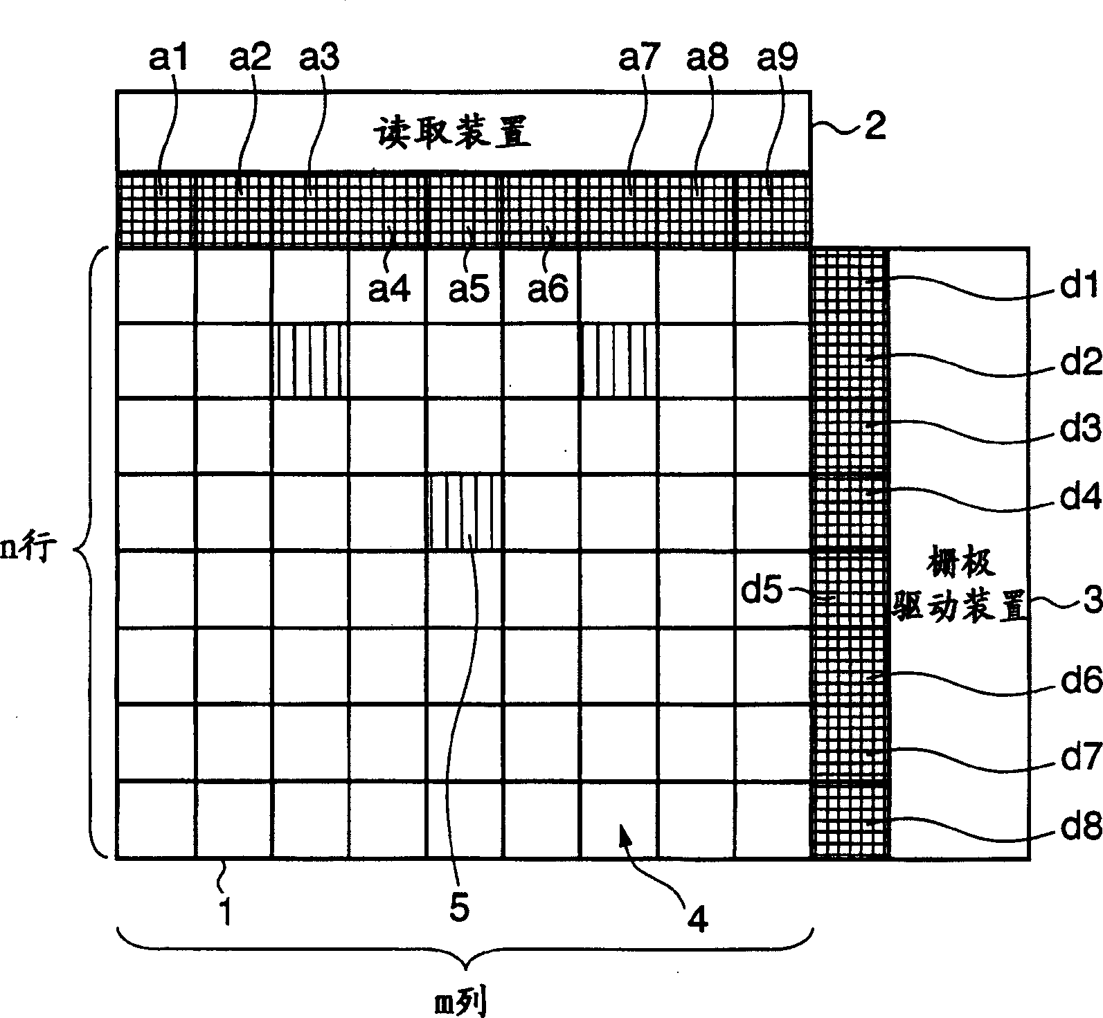
[0026] First, a first preferred embodiment of the present invention will be described. figure 1 It is a schematic diagram showing the layout of the radiation imaging apparatus according to the first preferred embodiment of the present invention.

[0027] In this embodiment, m columns and n rows of radiation detection pixels for imaging are arranged in a matrix on the insulating substrate 1 . In one radiation detection pixel for imaging, a conversion unit for converting radiation into an electric signal is provided, which is composed of a MIS type photoelectric conversion element (first semiconductor conversion element) and a thin film transistor (TFT) (switching element) for readout. M columns of radiation detection pixels for imaging are divided into, for example, 9 groups, and each group is connected to one of the TCPs a1 to a9 for reading. In addition, n rows of radiation detection pixels for imaging are divided into, for example, 8 groups, and each group is connected to ...

no. 2 Embodiment approach

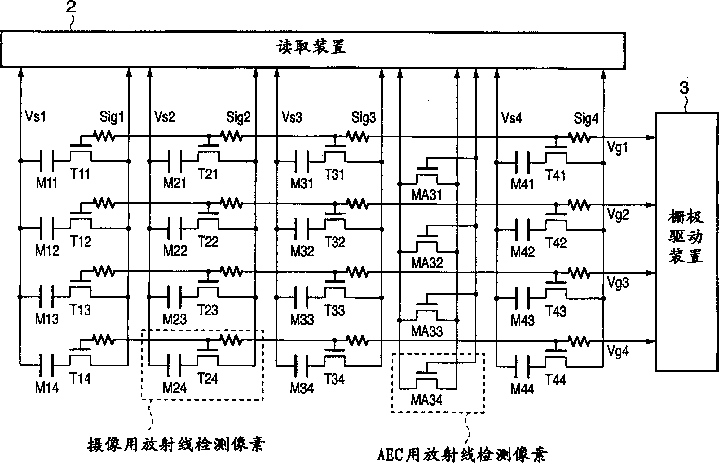
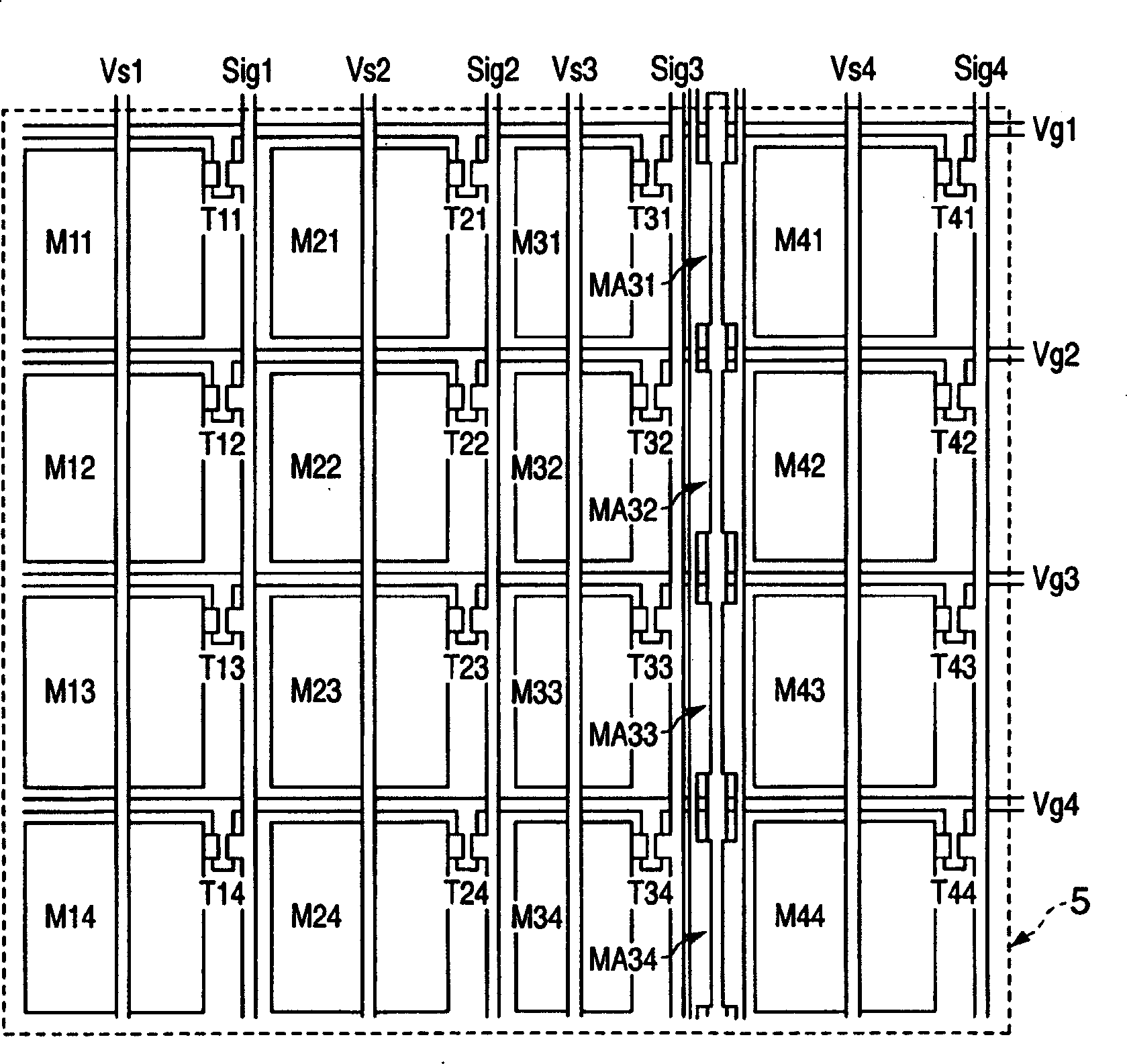
[0058] Next, a second preferred embodiment of the present invention will be described. Figure 5 It is a schematic diagram showing the layout of a radiation imaging apparatus according to a second preferred embodiment of the present invention.

[0059] In this embodiment, like the first embodiment, m columns and n rows of radiation detection pixels for imaging are arranged in a matrix on the insulating substrate 1 . The radiation detection pixels for imaging of m columns are divided into nine groups, for example. On the other hand, n rows of radiation detection pixels for imaging are divided into, for example, 8 groups, and each group is connected to one of the driving TCPs d1 to d8 . Of the radiation detection pixels for imaging in m columns divided into 9 groups, one of the pixels connected to the TCPs d1 to d4 for driving is connected to one of the TCPs a1 to a9 for reading, and to one of the TCPs d5 to d4 for driving. One of the pixels of d8 is connected to one of the TC...


PUM


Abstract

The radiation detection pixels for imaging in m rows and n columns are divided into, for example, 72 pixel areas, and the radiation detection pixels for imaging belonging to one pixel area are connected to the same TCP for reading and TCP for driving. In the above-mentioned 72 pixel areas, for example, in three areas (radiation detection areas for AEC), a plurality of radiation detection pixels for AEC are provided. In the radiation detection pixel for AEC, a TFT type sensor is provided. In addition, in each reading TCP, spare lines for radiation detection pixels for AEC are provided at both ends thereof, and by reading each spare line and connecting to a predetermined circuit in the device, the radiation detection pixels for AEC are connected to predetermined circuits. circuit to make the AEC circuit operate.

Description

technical field [0001] The present invention relates to a radiation imaging device and a radiation imaging system that are suitable for medical imaging diagnostic devices, non-destructive inspection devices, analysis devices using radiation, and the like. In addition, in this specification, it is assumed that electromagnetic waves such as visible light and X-rays are also included in radiation in addition to α-rays, β-rays, γ-rays, and the like. Background technique [0002] As a method of irradiating a subject with radiation and detecting the intensity distribution of the radiation passing through the subject to obtain a radiographic image of the subject, the following technology is currently being developed: using a tiny photoelectric conversion device A photoelectric conversion device in which pixels composed of , conversion elements, etc. are arranged in a grid to obtain digital images. In these radiation imaging apparatuses, acquired image data can be displayed in real...

Claims


Application Information

Patent Timeline
Patent Type & Authority Applications(China)
IPC IPC(8): G01T1/29G21K4/00H04N5/32
CPCG21K4/00H04N5/32G01T1/2928
Inventor 石井孝昌森下正和山崎达也辻井修平井明田村敏和野中秀树
Owner CANON KK
Why Eureka
Try Eureka