

Bandpass filter
A band-pass filter and channel technology, which is applied to waveguide-type devices, impedance networks, electrical components, etc., can solve problems such as difficulty in realizing sharp-cut band-pass filters and difficulty in realizing band-pass filters.
- Summary
- Abstract
- Description
- Claims
- Application Information
AI Technical Summary
Problems solved by technology
Method used
Image

Examples
Embodiment approach 1
[0055] Figure 10 is a plan view for explaining one mode of the filter according to the first embodiment of the present invention.
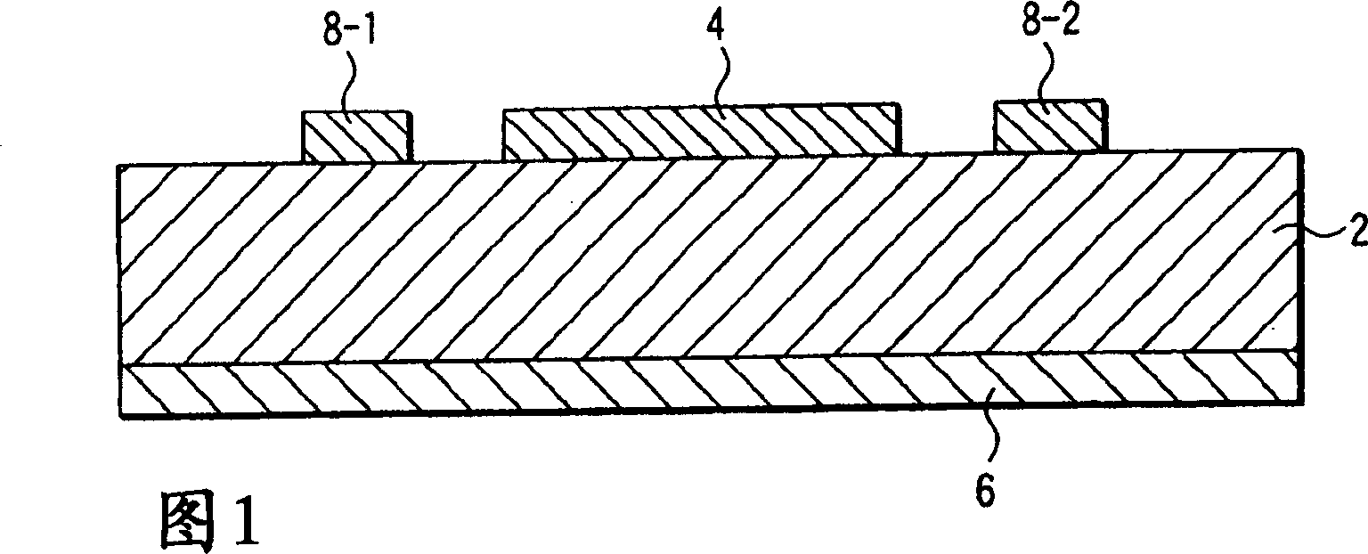
[0056] As in the description based on FIG. 1 , a superconducting microstrip line was formed on an MgO substrate 2 having a thickness of about 0.43 mm and a relative permittivity of about 10. Here, a Y-based copper oxide high-temperature superconducting thin film with a thickness of about 500 nm is used as the superconductor of the microstrip line, and the line width of the strip conductor is about 0.4 mm. This superconducting thin film can be formed by a laser deposition method, a sputtering method, a simultaneous deposition method, or the like.
[0057] Figure 10 The filter shown is of the Chebyshev type comprising six resonators 32, 34, 36, 38, 40 and 42 between input / output line paths 31 and 43 formed by excitation lines. These 6 half-wavelength hairpin resonators 32, 34, 36, 38, 40 and 42 whose opening sides face the same direction are ar...
Embodiment approach 2
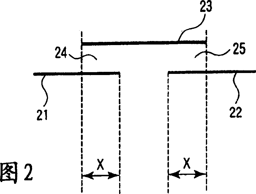
[0060] Figure 12 is a plan view illustrating one mode of a filter according to another embodiment of the present invention. Figure 12The filter shown is of the Chebyshev type comprising four resonators 51, 53, 55 and 57 between the input / output line paths 50 and 58 formed by the excitation lines. As the resonators, linear resonators 51, 53, 55, and 57 of one wavelength are used. Therefore, the wavelength corresponding to the resonant frequency is equal to the length of each resonator. In addition, the resonators 51, 53, 55 and 57 adjacent to each other are respectively bent as Figure 8 Wire vias 52, 54 and 56 of this shape are shown coupled. The length of each transmission line path 52, 54 and 56 is 7 / 4 wavelength, the length x of each coupled section is determined substantially as 1 / 4 wavelength, and this coupled section is arranged closest to the corresponding resonator. As mentioned above, since the length of each resonator is determined as one wavelength, the edges ...
Embodiment approach 3
[0064] Figure 14 is a plan view illustrating one mode of a filter according to still another embodiment of the present invention.
[0065] exist Figure 14 In the shown filter, a superconducting microstrip line via is formed on a MgO substrate (not shown) having a thickness of about 0.43 mm and a relative permittivity of 10. Here, a Y-based copper oxide high-temperature superconducting thin film with a thickness of about 500 nm is used as the superconductor of the microstrip line, and the line width of the strip conductor is about 0.4 mm. This superconducting thin film can be formed by a laser deposition method, a sputtering method, a simultaneous deposition method, or the like.
[0066] Figure 14 The shown filter is a four-stage filter consisting of four linear resonators 61, 63, 65 and 67 provided between input / output line paths 60 and 68 formed by excitation lines. exist Figure 14 In the filter shown, a resonator of one wavelength is used for each resonator, while a...
PUM
 Abstract
Description
Claims
Application Information